Cryogenic receiving amplifier and amplifying method
a cryogenic receiving amplifier and amplifier technology, applied in the direction of electroluminescent amplifiers, amplifiers with semiconductor devices only, amplifiers with semiconductor devices/discharge tubes, etc., can solve the problems of deteriorating the overall linearity of cryogenic receiving amplifiers and the inability to obtain a sufficiently high power added efficiency
- Summary
- Abstract
- Description
- Claims
- Application Information
AI Technical Summary
Benefits of technology
Problems solved by technology
Method used
Image
Examples
first embodiment
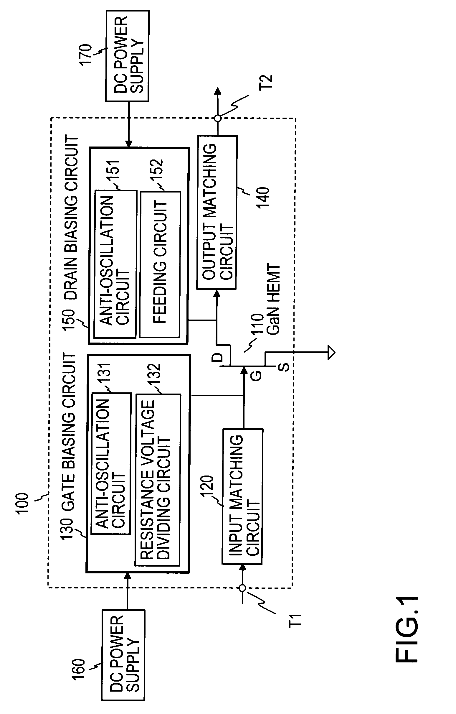
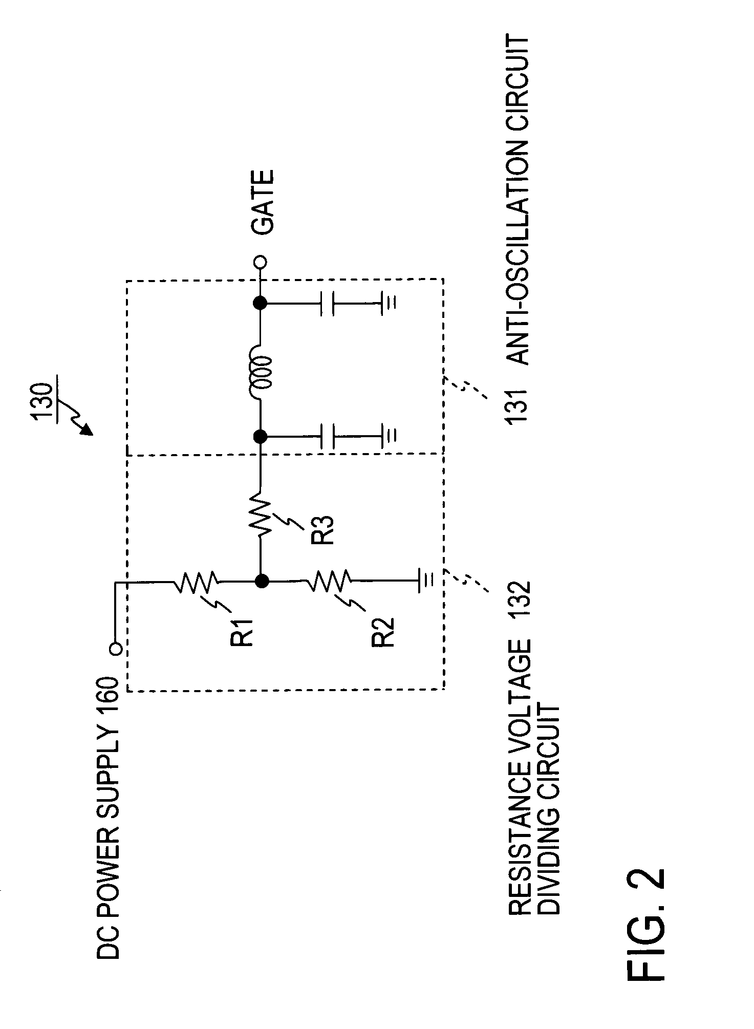
[0046]FIG. 1 shows a configuration of a cryogenic receiving amplifier 100 according to the first embodiment of the present invention. In the configuration, a GaN HEMT 110 is employed as an amplifying device. The cryogenic receiving amplifier 100 includes an input matching circuit 120 which makes an impedance matching between the gate of the GaN HEMT 110 and an external apparatus connected to an input terminal T1 of the cryogenic receiving amplifier 100, a gate biasing circuit 130 which applies a DC voltage to the gate of the GaN HEMT 110, an output matching circuit 140 which makes an impedance matching between the drain of the GaN HEMT 110 and an external apparatus connected to an output terminal T2 of the cryogenic receiving amplifier 100, and a drain biasing circuit 150 which applies a DC voltage to the drain of the GaN HEMT 110.
[0047]The input matching circuit 120 and the output matching circuit 140 are designed for operation at 2 GHz, for example. The input matching circuit 120 ...
second embodiment
[0066]FIG. 15 shows a configuration of a two-stage receiving amplifier with a cryogenic receiving amplifier 100 of the present invention disposed at the second stage. On the first stage is disposed a cryogenic receiving amplifier 200 employing a GaAs HEMT 210 having a low noise figure. The first stage cryogenic receiving amplifier 200 may be mounted, for example, on the cooling stage 921 inside the vacuum chamber 910 shown in FIG. 14, and connected in series between the superconducting filter 950 and the cryogenic receiving amplifier 100. As shown in the above-mentioned non-patent literature 5 , the GaAs HEMT 210 at the first stage has such characteristics as a noise figure of 0.3 dB and a gain of 10 dB. For example, the GaN HEMT 110 at the second stage may be designed to have such characteristics as the noise figure of 2 dB and the gain of 26 dB, resulting in the noise figure of about 0.53 dB in the entire configuration of FIG. 15. Thus, as compared with the three-stage cryogenic r...
third embodiment
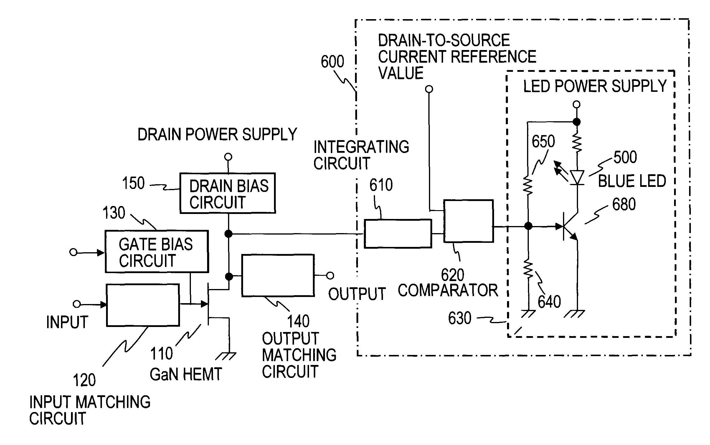
[0068]In the third embodiment, it is contemplated to improve the reduction in drain-to-source current of a GaN HEMT 110 due to the current collapse phenomenon which is generated in a cryogenic temperature environment. In the current collapse phenomenon due to the cryogenic temperature environment, after the electron-excited state is frozen, the number of excited electrons is increased with time. Hence, even if a gate biasing voltage is set, it is impossible to avoid a phenomenon in which a drain current gradually increases or decreases.
[0069]Incidentally, it is generally known that an illumination of a semiconductor with light causes a change in characteristic of the semiconductor. This is observed because light energy is injected into the semiconductor to activate excitation of electrons. The injected light energy relates to the band gap of the semiconductor and the wavelength of the injected light. However, the wavelength of the light effective on the GaN HEMT 110 has not been fou...
PUM
 Abstract
Description
Claims
Application Information
 - R&D
- Intellectual Property
- Life Sciences
- Materials
- Tech Scout
- Unparalleled Data Quality
- Higher Quality Content
- 60% Fewer Hallucinations
Browse by: Latest US Patents, China's latest patents, Technical Efficacy Thesaurus, Application Domain, Technology Topic, Popular Technical Reports.
© 2025 PatSnap. All rights reserved.Legal|Privacy policy|Modern Slavery Act Transparency Statement|Sitemap|About US| Contact US: help@patsnap.com


