Circuit module and electrical component

a technology of circuit modules and electrical components, applied in the direction of printed circuit aspects, sustainable manufacturing/processing, final product manufacturing, etc., can solve the problems of increasing impedance and longer wiring length, and achieve the effect of suppressing the increase in the total length of the shared signal line, and reducing the cost of production

Active Publication Date: 2010-07-27
MICRON TECH INC
View PDF14 Cites 0 Cited by
  • Summary
  • Abstract
  • Description
  • Claims
  • Application Information

AI Technical Summary

Benefits of technology

[0020]That is, when the fly-by system is adopted, wiring capacitances and inductances of packages or input / output circuits of the devices are increased at each point of connection of the devices. This brings about a large variation of impedance. The present invention aims to suppress the deterioration of the signal quality by lowering the variation of impedance. Specifically, the stacking of devices has been mainly used so far for the high-density mounting, but is disadvantageous in that a greater variation of impedance takes place on a shared signal pin, in comparison with the case of the non-stacking.
[0035]According to the present invention, in the circuit module in which the above-mentioned electrical components are arranged in the staggered manner, a wiring length of the shared signal line does not double. Also, intervals for connection are made half. This serves to prevent an increase in the total length of the shared signal line. As a result, the deterioration of the signal quality due to the increase in wiring length of the shared signal line can be suppressed. Further, according to the present invention, the stacking is unnecessary and thus a package in which a distance from a circuit board to an input / output circuit of a device is short can be employed, so a wiring capacity in the package and the inductance are reduced to suppress the deterioration of the signal quality in the package. As described above, the capacity and the inductance can be reduced, so attenuation of a waveform is reduced even in a high frequency region. Also, with a reduction in impedance variation in the shared signal line on the circuit board, it is possible to lower occurrence of a reflected wave at an impedance unmatched point.
[0036]Moreover, the area of the substrate connecting portion connected to a circuit board (for example, mother board or memory module substrate) is made smaller than the area of a solid-state circuit element so that adjacent solid-state circuit elements can be opposed to each other. Accordingly, the staggered mounting in the height direction is enabled on the circuit board, and the degree of lowering the mounting density can be reduced. Under specific conditions, the mounting density similar to that of the stacked package is also enabled. Conventionally, only a component thinner than a diameter of a solder ball has been mounted close to a pin of a signal line. However, as a secondary advantage, the application of the present invention allows a component thicker than the diameter of a solder ball to be mounted close to the pin of the signal line. Further, the width of the substrate connecting portion is made narrow, and thus the cost thereof can be reduced.

Problems solved by technology

This inevitably makes the wiring length longer and results in an increase of impedance.

Method used


Image

  • Circuit module and electrical component
  • Circuit module and electrical component
  • Circuit module and electrical component

Examples


first embodiment

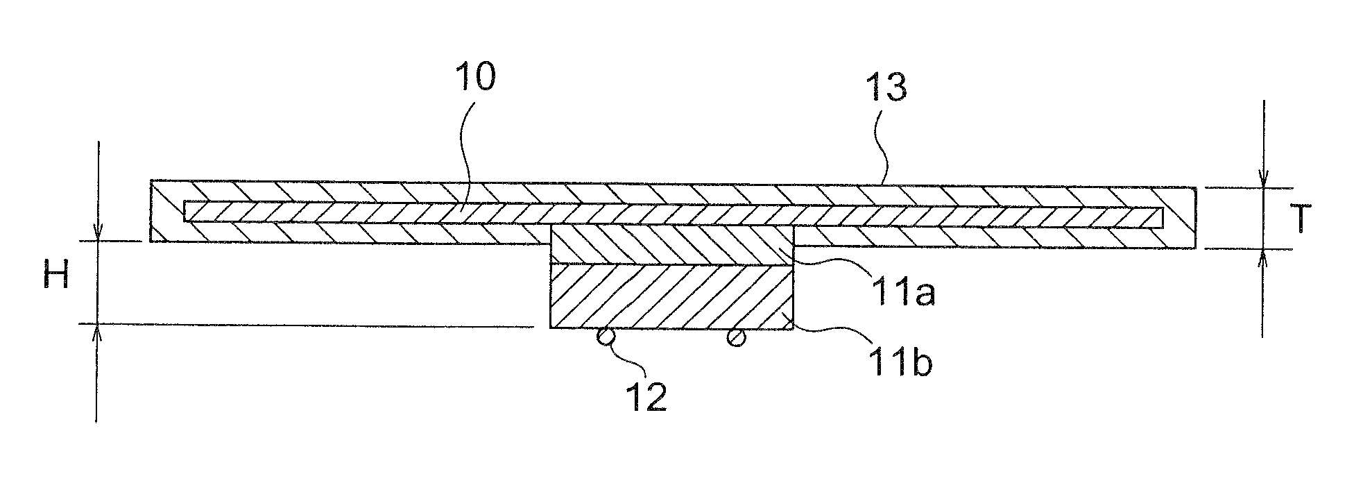
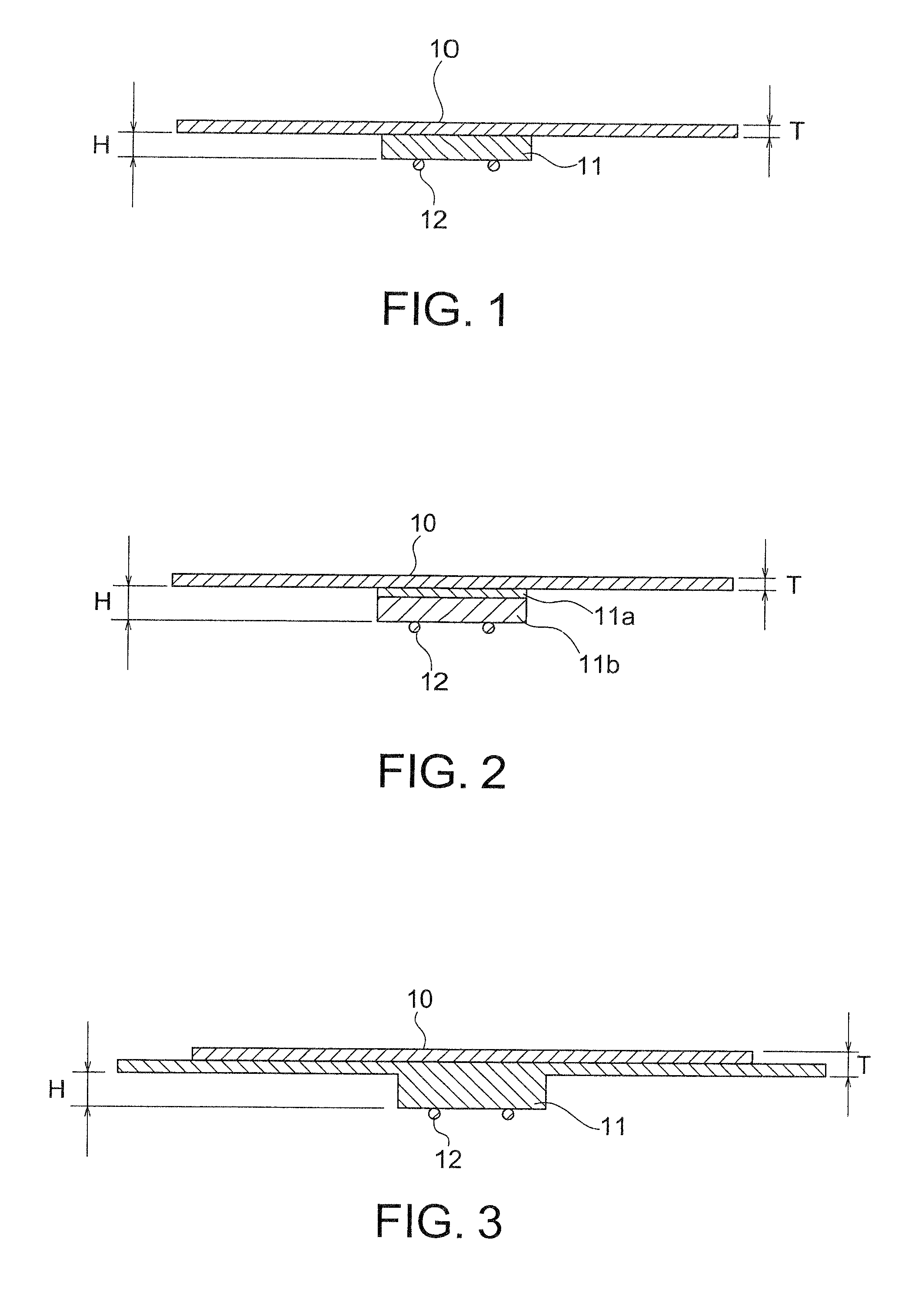
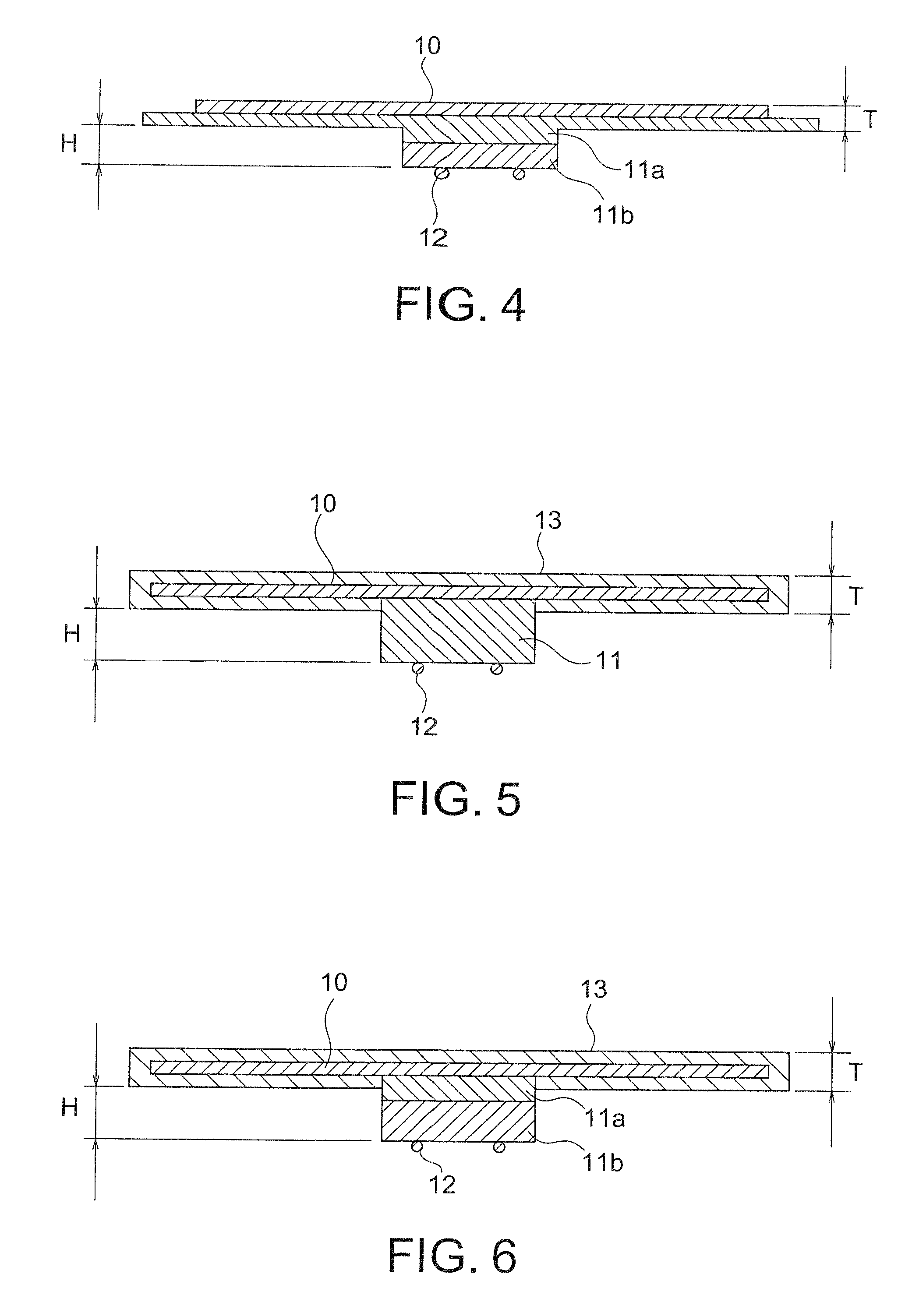
[0053]Referring to FIG. 1, an electrical component according to the present invention has a solid-state circuit portion 10 including, as a base substance, a semiconductor such as silicon, and a substrate connecting portion 11 provided to a lower surface of the solid-state circuit portion 10. As illustrated in FIG. 1, the substrate connecting portion 11 has an area smaller than that of the solid-state circuit portion 10. The substrate connecting portion 11 has an upper surface electrically connected to the solid-state circuit portion 10 and a lower surface connected to an external substrate (that is, circuit board (not shown)). In other words, the solid-state circuit portion 10 has a lower surface which is opposed to the substrate connecting portion 11 and which has a support surface supported by the substrate connecting portion 11 and an opposing surface placed outside of the support surface. The opposing surface has a wide area enough to be opposed to another electrical component.

[...

second embodiment

[0063]Referring to FIGS. 9 and 10, there are shown a side view and a front view of a circuit module according to the present invention, respectively. In the illustrated circuit module, a plurality of electrical components are mounted on a circuit board 14 in addition to a logical circuit 15 such as a controller. In the example shown in the figures, electrical components different from each other in height are arranged on the front surface and back surface of the circuit board 14 in the height direction in the staggered manner so as to partially oppose adjacent electrical components to each other. That is, in the example shown in the figures, of the electrical components shown in FIGS. 1 to 8, electrical components including the substrate connecting portions 11 and 11a which are different from each other in height are alternately arranged on the circuit board 14. Also, in FIG. 9, a circuit element (for example, capacitor) 16 whose height is higher than that of the solder ball 12 is a...

third embodiment

[0068]Referring to FIG. 15, there is shown a circuit module according to the present invention, in which substrate connecting portions 11a to 11e are connected to portions which are not center portions of solid-state circuit portions 10a to 10e. In the example shown in the figure, the substrate connecting portions 11a, 11c, and 11e are provided to the portions located close to the left ends of the solid-state circuit portions 10a, 10c, and 10e, respectively. Meanwhile, the substrate connecting portions 11b and 11d are provided to the portions located close to the right ends of the solid-state circuit portions 10b and 10d, respectively. Further, the substrate connecting portions 11b and 11d are higher than the other substrate connecting portions 11a, 11c, and 11e. In this embodiment, a structure in which two tapes, substrates, or the like, are laminated is adopted and therefore the staggered arrangement is enabled.

[0069]In addition, the embodiment shown in the figure has been describ...


PUM


Abstract

In an electrical component including a solid-state circuit portion and a substrate connecting portion, the solid-state circuit portion includes: a supporting surface faced to and supported by the substrate connecting portion; and an opposing surface which is widened outside the supporting surface and which has an area enough to be opposed to another solid-state circuit portion. This structure makes it possible to arrange, on a circuit board, a plurality of the electrical components in a staggered manner in a height direction.

Description

[0001]This application is based upon and claims the benefit of priority from Japanese patent application No. 2007-187258, filed on Jul. 18, 2007, the disclosure of which is incorporated herein in its entirety by reference.BACKGROUND OF THE INVENTION[0002]1. Field of the Invention[0003]The present invention relates to a circuit module which is operated at a high-speed operation and which is mounted in a high density, and an electrical component used for the circuit module.[0004]2. Description of the Related Art[0005]A high speed operation and a high density mounting have been required of a circuit module, such as a memory module. As an economical high-density mounting technology, recent interest has been mainly directed to stacking solid-state circuit elements in order to mount the circuit module in a high density. In a silicon semiconductor which has presently mainly been used, a proposal has been offered about a technology which perforates a silicon substrate itself to connect uppe...

Claims


Application Information

Patent Timeline
Patent Type & Authority Patents(United States)
IPC IPC(8): H01L23/053
CPCH01L23/3114H01L25/0657H05K1/181H01L23/3128H01L2924/30107H01L24/48H05K2201/10515H01L25/105H01L2224/16H01L2224/48091H01L2225/0651H01L2225/06517H01L2225/06527H01L2225/06582H01L2225/06586H01L2924/19041H01L2924/3011H05K2201/09709H01L2924/00014H01L2924/00H01L2924/181H01L2924/15311Y02P70/50H01L2924/00012H01L2224/45099H01L2224/45015H01L2924/207
Inventor ONO, TAKAO
Owner MICRON TECH INC
Why Eureka
Try Eureka