
Post-lithography misalignment correction with shadow effect for multiple patterning

a post-lithography and patterning technology, applied in the direction of basic electric elements, semiconductor/solid-state device manufacturing, electric devices, etc., can solve the problems of long development time for high-throughput manufacturing applications, severe challenge to significantly reduce the misalignment budget in the lithographic process, and serious challenges to process yield and circuit design/layou

Inactive Publication Date: 2010-04-20
CHEN YIJIAN
View PDF1 Cites 11 Cited by
  • Summary
  • Abstract
  • Description
  • Claims
  • Application Information

AI Technical Summary

Problems solved by technology

However, all these NGL technologies face their own technological challenges and still need a long development time before their applications in high-throughput manufacturing.
It is a severe challenge to significantly reduce the misalignment budget in a lithographic process to meet the multiple-patterning requirement at 32 nm half pitch and below.
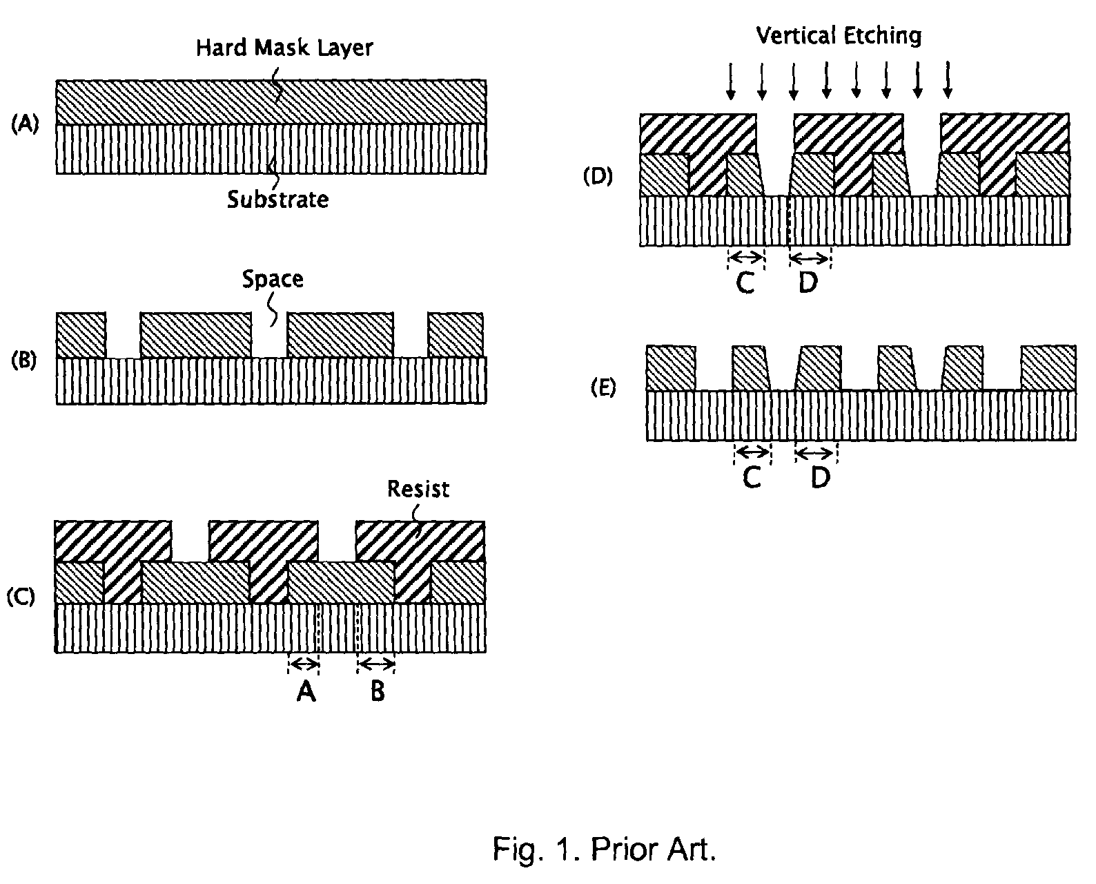
However, as shown in FIG. 1(C), the trench is not located right at the center of the line (e.g., A≠B) due to an unavoidable misalignment during a lithographic process.
This results in unequal width of the final dense features (e.g., length C≠D) and brings serious challenges to process yield and circuit design / layout.
Similar problem exists in a multiple-patterning process to obtain dense features with their pitch reduced to ⅓, ¼, .
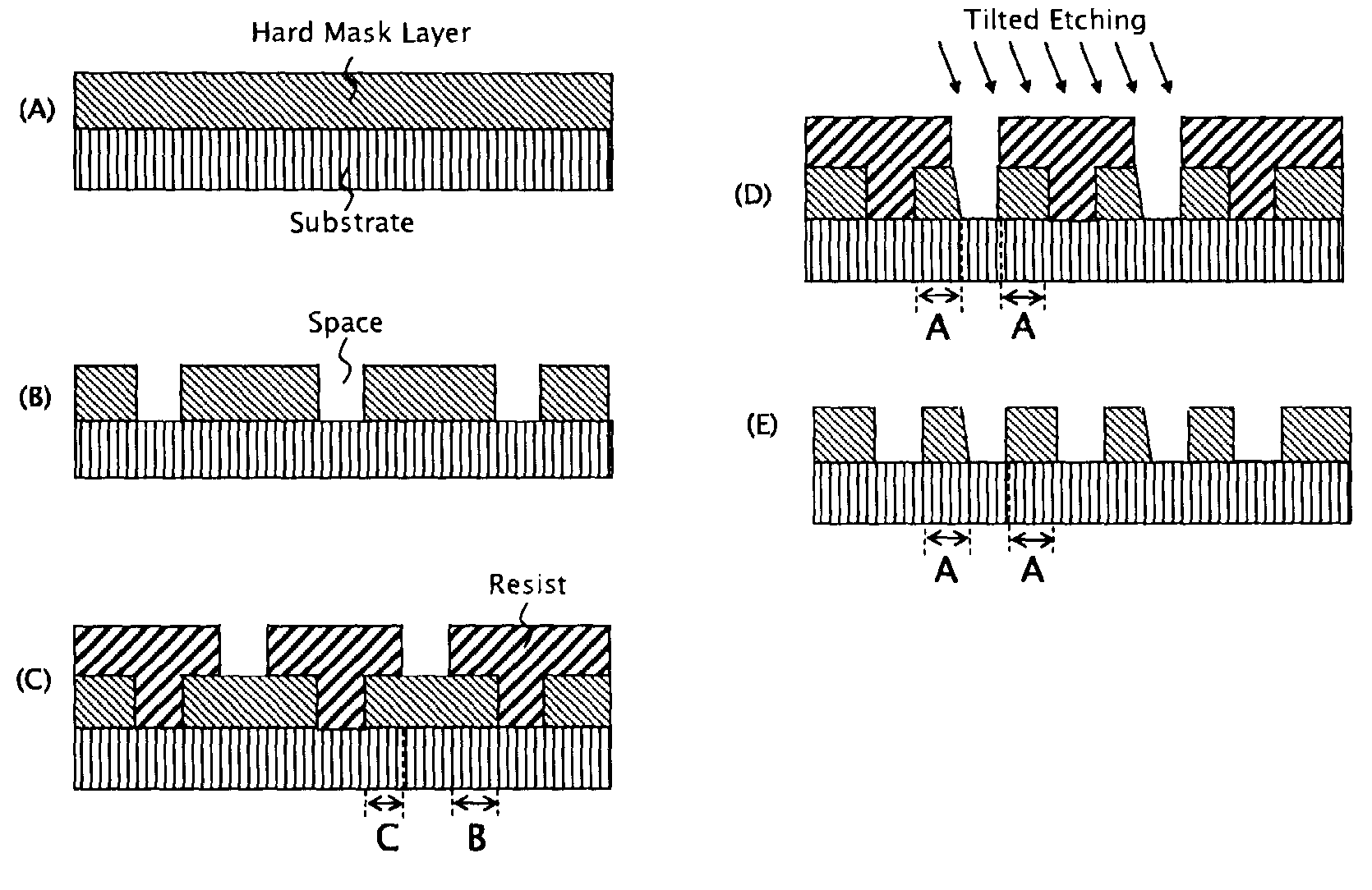
First, the slope of left side walls of the etched structures becomes more vertical while the opposite happens to the slope of right side walls, which results in asymmetric final structures.

Method used


Image

  • Post-lithography misalignment correction with shadow effect for multiple patterning
  • Post-lithography misalignment correction with shadow effect for multiple patterning
  • Post-lithography misalignment correction with shadow effect for multiple patterning

Examples


Embodiment Construction

[0018]If the misalignment can be measured right after the exposed resist is developed and baked, then the correction process is shown in FIG. 5. The tilting angle can be arbitrary (2-D) and should be adjusted according to measured values of misalignment in both X and Y directions; but here we only use the right-tilted etching as an example to demonstrate the concept. First, we put a hard mask on top of the substrate and pattern this hard-mask layer with semi-dense features wherein the size of lines is three times of the size of spaces as shown in FIG. 5(A) and FIG. 5(B). In step 5(C), resist is spun on the patterned hard-mask layer and exposed again to print another pattern of semi-dense features with its position shifted. Ideally, we would like to shift the second pattern in such a way that the trenches in the resist will be located right at the center of the corresponding line structures underneath. However, due to misalignment in a lithographic process, perfect overlay can not be...


PUM


Abstract

Misalignment created during a multiple-patterning process is a serious challenge for critical dimension (CD) control and layout design in continuing integrated-circuit device scaling. A number of post-lithography misalignment correction technologies based on the shadow effect are invented for multi-patterning lithographic applications. When applied to transfer patterns from a top layer to an underneath layer, the subtractive shadow effect in anisotropic plasma etching combined with a hard-mask process, will shift the position of features such that the previously produced misalignment can be corrected. Also, additive shadow effect in a sputtering / evaporation process can be used. Misalignment correction methods allow the semiconductor industry to print sub-32 nm (half-pitch) features using the double-patterning technique with currently existing lithographic tools (e.g., 193-nm DUV scanner), therefore postponing the need of expensive next-generation lithography (NGL). The misalignment correction methods can be applied to existing lithography technologies to print features smaller than their physical resolution limits.

Description

BACKGROUND OF THE INVENTION[0001]Optical DUV (deep ultraviolet, 193 nm) immersion lithography with NA≈1.3 has the capability of printing half-pitch features down to about 40 nm. The potential next-generation lithography (NGL) technologies include EUV (extreme ultraviolet), maskless, and nano-imprint lithography [1]. However, all these NGL technologies face their own technological challenges and still need a long development time before their applications in high-throughput manufacturing. Recently, double patterning has attracted much industrial interest which prints less dense line / space or contact hole patterns twice on the same wafer to finally obtain dense patterns with double spatial frequency [2]. In principle, a similar multiple-patterning concept can be developed but both need extremely high alignment accuracy. It is a severe challenge to significantly reduce the misalignment budget in a lithographic process to meet the multiple-patterning requirement at 32 nm half pitch and ...

Claims


Application Information

Patent Timeline
IPC IPC(8): H01L21/336H01L21/302H01L21/461
CPCH01L21/0337H01L21/76816H01L21/31144H01L21/0338
Inventor CHEN, YIJIAN
Owner CHEN YIJIAN
Learn More