
Deposition of tungsten nitride

a technology of tungsten nitride and pnl, which is applied in the direction of chemical vapor deposition coating, coating, metallic material coating process, etc., can solve the problems of poor step coverage in high aspect ratio trenches, vias and contacts, and the wide application of wn, so as to achieve good tungsten nitride adhesion to the substrate, good step coverage, and fine control of deposition thickness

Active Publication Date: 2010-04-06
NOVELLUS SYSTEMS
View PDF60 Cites 83 Cited by
  • Summary
  • Abstract
  • Description
  • Claims
  • Application Information

AI Technical Summary

Benefits of technology

This method enables the deposition of tungsten nitride with improved adhesion to dielectric surfaces and conformal coverage in high aspect ratio features, suitable for advanced semiconductor applications, while maintaining low processing temperatures.

Problems solved by technology

A key limitation that has prevented wider application of WN in the past has been poor step coverage in high aspect ratio trenches, vias and contacts.
Conventional physical vapor deposition (PVD) techniques are not able to meet these criteria.
Although standard tungsten nitride CVD techniques can provide good step coverage and adequately fill low aspect ratio features (e.g., <5:1 aspect ratio), as semiconductor fabrication technology approaches the nanometer scale, the demands for step coverage and gap filling are becoming more stringent and CVD may not be suitable for the task.
Traditional plasma-enhanced CVD of tungsten nitride has relatively poor step coverage for a CVD process (<50% SC in a 5:1 aspect ratio cylindrical contact).
This is not adequate for the demands of current and future semiconductor technology with aspect ratios exceeding 10 to 1 and critical dimensions less than 100 nanometers.
Finally, the high deposition temperatures required by many TiN deposition techniques (e.g. PECVD-TiN from TiCl4) require high deposition temperatures that are incompatible with low-K dielectrics or nickel silicide.

Method used


Image

  • Deposition of tungsten nitride
  • Deposition of tungsten nitride
  • Deposition of tungsten nitride

Examples


Embodiment Construction

[0022]Introduction

[0023]As indicated, the present invention provides methods for depositing a tungsten nitride layer, especially for applications in which the tungsten nitride is deposited over dielectric surfaces and wherein thin, conformal and adhesive layers are required. Preferred methods involve pulsed nucleation layer (PNL) deposition techniques, which will be described in detail below.

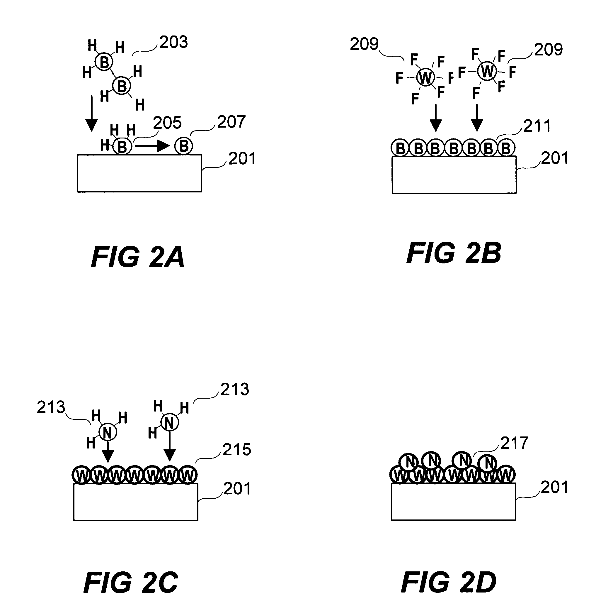
[0024]One preferred approach to the PNL process involves first depositing diborane (or other boron-containing precursor) on a substrate surface to form a “sacrificial” boron-containing layer. This sacrificial layer subsequently reacts with a tungsten precursor to form tungsten. The diborane deposition process is not a conventional self-limiting ALD type deposition process. Rather, the diborane reacts on the dielectric surface to decompose into a boron film. The reaction can proceed as long as the substrate is continually exposed to diborane. However, to ensure that a limited amount of tungsten i...


PUM

PropertyMeasurementUnit
processing temperaturesaaaaaaaaaa
coverageaaaaaaaaaa
critical dimensionsaaaaaaaaaa

Abstract

Methods for depositing a tungsten nitride layer are described. The methods form a tungsten nitride layer using a carefully controlled deposition technique such as pulsed nucleation layer (PNL). Initially, a tungsten layer is formed on a substrate surface. The tungsten layer is then exposed to a nitriding agent to form a tungsten nitride layer. Methods of forming relatively thick layers of involve repeated cycles of contact with reducing agent, tungsten precursor and nitriding agent. In some cases, the cycle may also include contact with a dopant precursor such as phosphine or arsine.

Description

CROSS-REFERENCE TO RELATED PATENT APPLICATIONS[0001]This application is a divisional application of and claims priority from U.S. patent application Ser. No. 10 / 690,492, filed on Oct. 20, 2003, now U.S. Pat. No. 7,005,372 entitled “DEPOSITION OF TUNGSTEN NITRIDE,” by Karl B. Levy et al. as inventors; which claims priority under 35 USC 119(e) from U.S. Provisional Patent Application No. 60 / 441,834 filed Jan. 21, 2003, naming Fair et al. as inventors, which are incorporated herein by reference in its entirety. This application is also related to the U.S. application Ser. No. 09 / 975,074 (issued as U.S. Pat. No. 6,635,965) filed Oct. 9, 2001, entitled ULTRA THIN TUNGSTEN LAYER WITH IMPROVED STEP COVERAGE, by Lee et al., and U.S. application Ser. No. 10 / 649,351, filed Aug. 26, 2003, entitled METHOD FOR REDUCING TUNGSTEN FILM ROUGHNESS AND IMPROVING STEP COVERAGE, by Lee et al., which is incorporated herein by reference for all purposes.FIELD OF THE INVENTION[0002]This invention pertains ...

Claims


Application Information

Patent Timeline
Patent Type & Authority Patents(United States)
IPC IPC(8): H01L21/44C23C16/02C23C16/34C23C16/44C23C16/455H01L21/285
CPCC23C16/0272C23C16/34H01L21/28562C23C16/45534C23C16/4554C23C16/45531H01L21/76843
Inventor LEVY, KARL B.SUNG, JUNGHWANASHTIANI, KAIHAN A.FAIR, JAMES A.COLLINS, JOSHUAGAO, JUWEN
Owner NOVELLUS SYSTEMS
Learn More