
Rework process for photoresist film

a rework process and film technology, applied in the field of rework process for a, can solve the problems of wasting time and manpower for producing the substrate, unable to form a resist pattern, etc., and achieve the effects of reducing cost, reducing labor intensity, and reducing labor intensity

Inactive Publication Date: 2009-12-29
SHIN ETSU CHEM IND CO LTD
View PDF11 Cites 2 Cited by
  • Summary
  • Abstract
  • Description
  • Claims
  • Application Information

AI Technical Summary

Benefits of technology

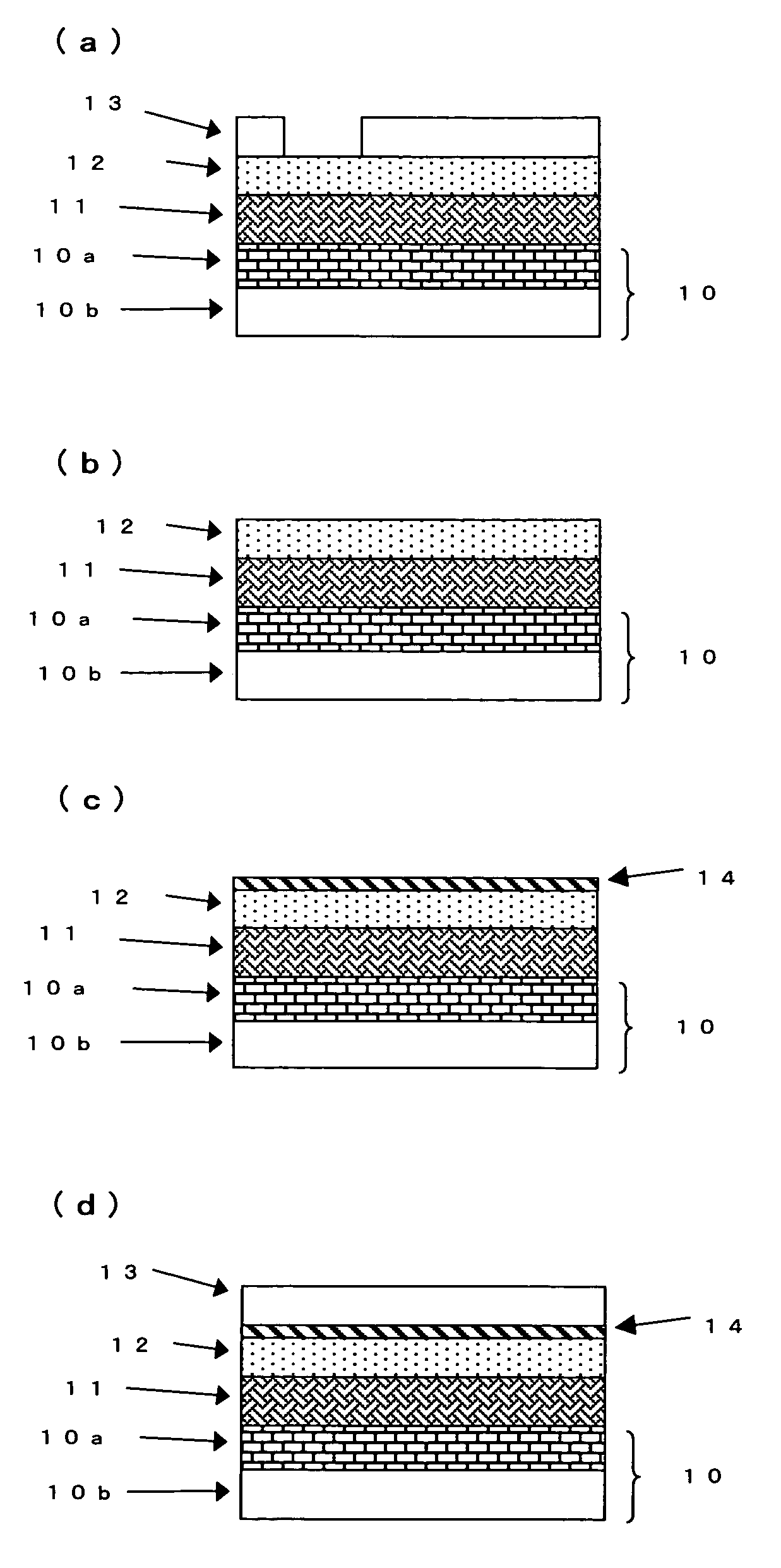
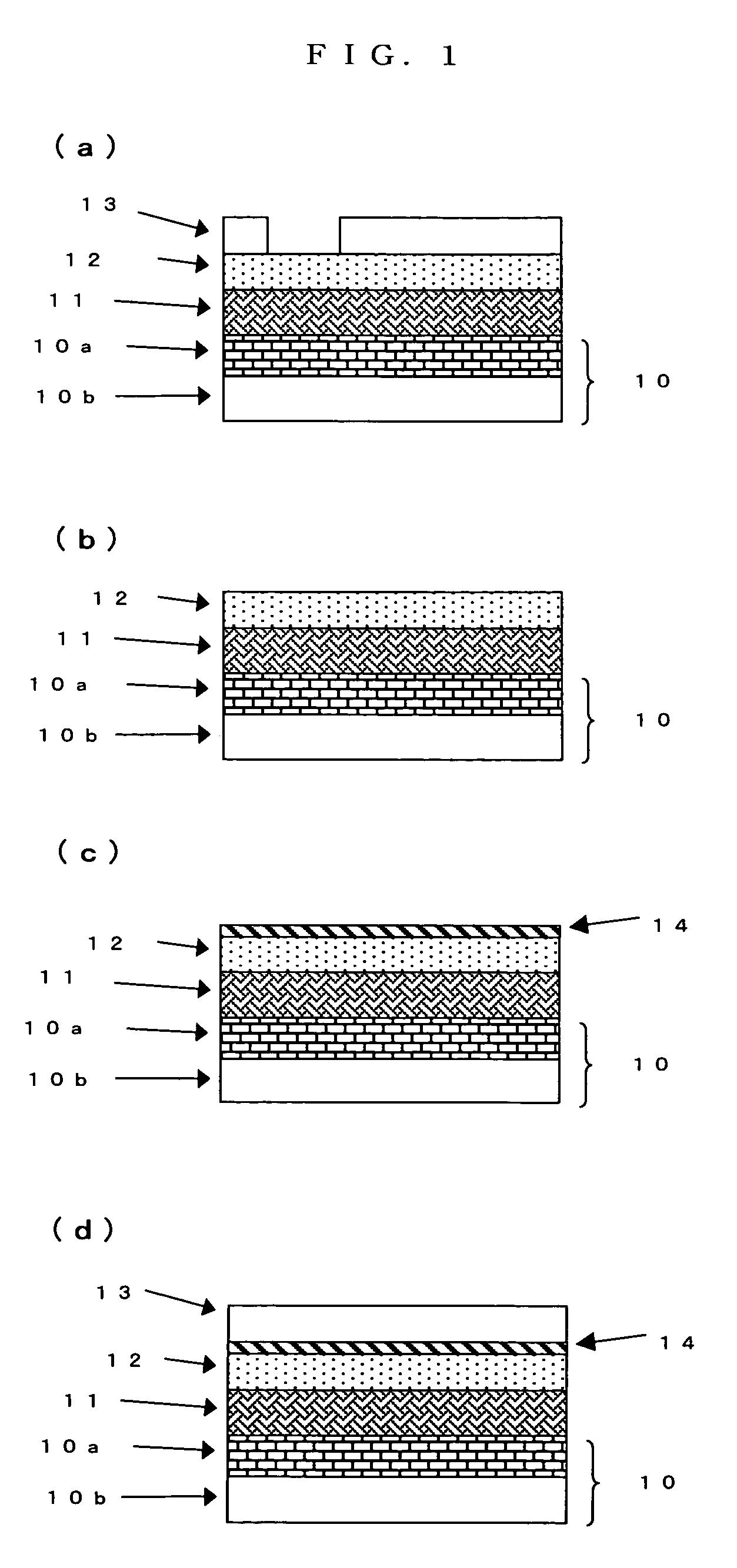
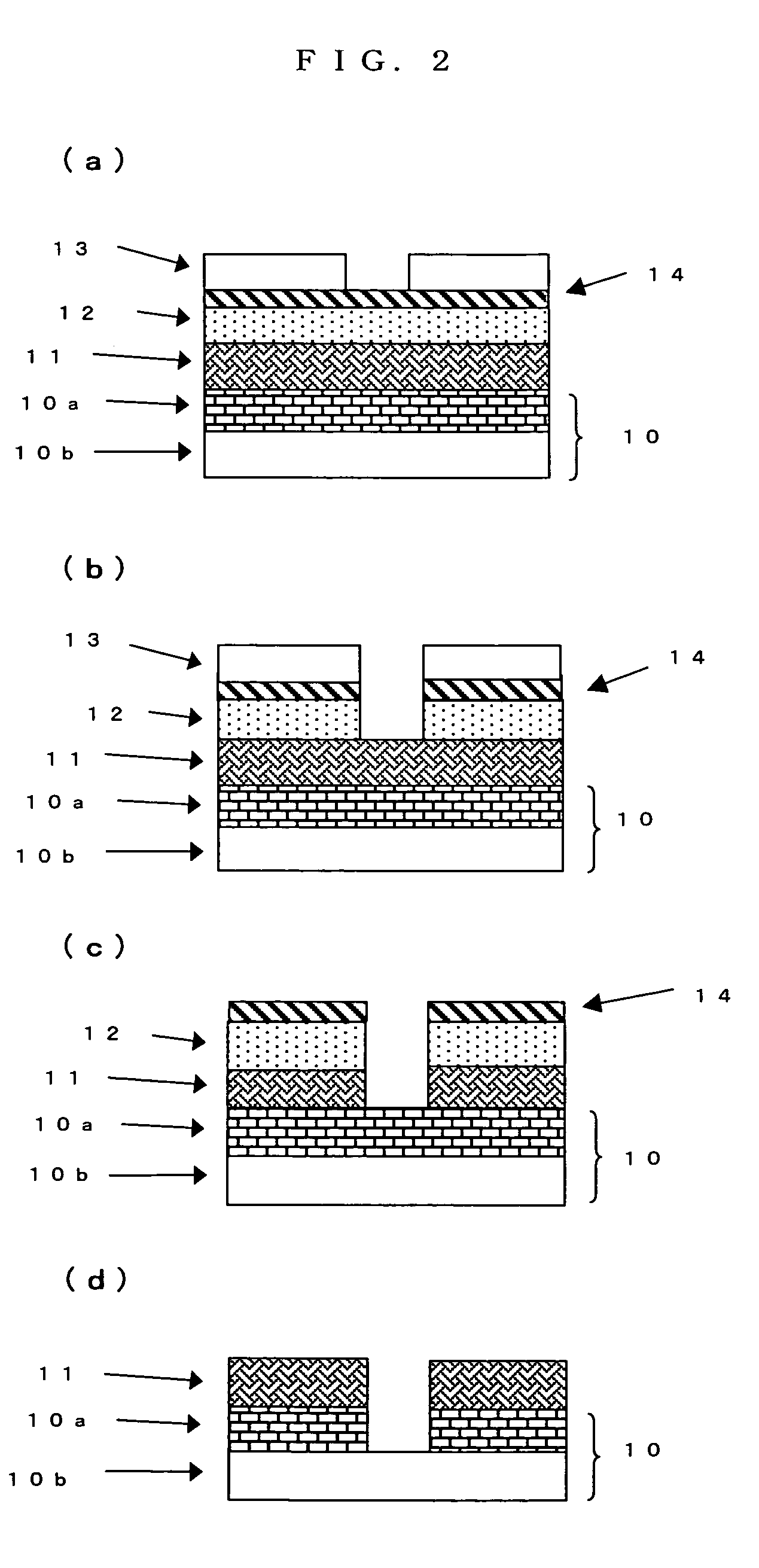
The present invention provides a rework process for a photoresist film that can be conducted more easily at lower cost and provide an excellent resist pattern. The rework process involves removing the photoresist film with a solvent while leaving the first silicone resin film unremoved, forming a second antireflection silicone resin film over the first silicone resin film, and re-forming the photoresist film over the second silicone resin film. This allows for easier re-formation of the photoresist film and ensures an excellent resist pattern. The substrate can also have an organic film under the first silicone resin film, which further enhances the resist pattern. The invention also provides a patterning process using the rework process and a substrate with a pattern formed using the rework process.

Problems solved by technology

In the above process, formation of a resist pattern can fail because striation is generated when a resist solution is applied, or deviation is generated in the resist pattern after exposure.
In such a case of failure, transferring a pattern down to a substrate with a deviated resist pattern produces a failed substrate and also wastes time and manpower expended for producing the substrate.

Method used


Image

  • Rework process for photoresist film
  • Rework process for photoresist film
  • Rework process for photoresist film

Examples


example 1

[Preparation of Silicone Resin Film Composition]

[0202]In a 3000 ml glass flask, 1400 g of ethanol, 700 g of pure water, and 50 g of aqueous solution of 25 mass % tetramethylammonium hydroxide were placed, and stirred. To this mixture, a mixture of 139 g of 2-(3,4-epoxycyclohexyl)ethyl trimethoxy silane and 32 g of phenyl trimethoxy silane was added dropwise at a liquid temperature of 40 degrees C. After that, the solution was stirred for 2 hours at 40 degrees C. After the reaction finished, the reaction was quenched by adding 35 g of acetic acid, and ethanol was removed under a reduced pressure. To thus-obtained solution, 2000 ml of ethyl acetate was added and a water layer was separated. An organic layer was washed twice with ultrapure water. To this contents, 600 g of propylene glycol monomethyl ether acetate (PGMEA) was added, and the contents were heated up to a liquid temperature of 40 degrees C. under a reduced pressure to give Polymer 1.

[0203]Mass-average molecular weight (Mw...


PUM

PropertyMeasurementUnit
sizeaaaaaaaaaa
wavelengthaaaaaaaaaa

Abstract

There is disclosed a rework process for a photoresist film over a substrate having at least a first antireflection silicone resin film and the photoresist film over the first silicone resin film comprising: at leastremoving the photoresist film with a solvent while leaving the first silicone resin film unremoved;forming a second antireflection silicone resin film over the first silicone resin film; andforming a photoresist film again over the second silicone resin film. There can be provided a rework process for a photoresist film that can be conducted more easily at lower cost and provide more certainly an excellent resist pattern.

Description

BACKGROUND OF THE INVENTION[0001]1. Field of the Invention[0002]The present invention relates to a rework process for a photoresist film over a substrate having an antireflection silicone resin film and a photoresist film over the silicone resin film.[0003]2. Description of the Related Art[0004]With a tendency of realizing high integration and high-speed of LSI, a finer pattern rule has been demanded in recent years. The lithography technique with optical exposure, which is used for general purpose at present, is reaching an inherent limiting resolution derived from a wavelength of a light source.[0005]There is widely used optical exposure using g line (436 nm) or i line (365 nm) of a mercury-vapor lamp as a light source for lithography when a resist pattern is formed. It has been considered that a method of using an exposure light with a shorter wavelength is effective as a means for obtaining a further finer pattern. For this reason, KrF excimer laser (248 nm) with a short wavelen...

Claims


Application Information

Patent Timeline
Patent Type & Authority Patents(United States)
IPC IPC(8): G03F7/00G03F1/00G03F7/004G03F7/11H01L21/027
CPCG03F7/0752G03F7/168G03F7/091G03F7/422G03F7/11G03F7/26G03F7/00
Inventor OGIHARA, TSUTOMUUEDA, TAKAFUMI
Owner SHIN ETSU CHEM IND CO LTD
Learn More