
Gate-enhanced junction varactor

a technology of gate-enhanced junctions and varactors, which is applied in the direction of oscillator generators, diodes, semiconductor devices, etc., can solve the problems of relatively complex process for manufacturing integrated circuit components, complicated process, etc., and achieve the effect of high maximum-to-minimum varactor capacitance ratio

Inactive Publication Date: 2009-08-25
NAT SEMICON CORP
View PDF27 Cites 21 Cited by
  • Summary
  • Abstract
  • Description
  • Claims
  • Application Information

AI Technical Summary

Benefits of technology

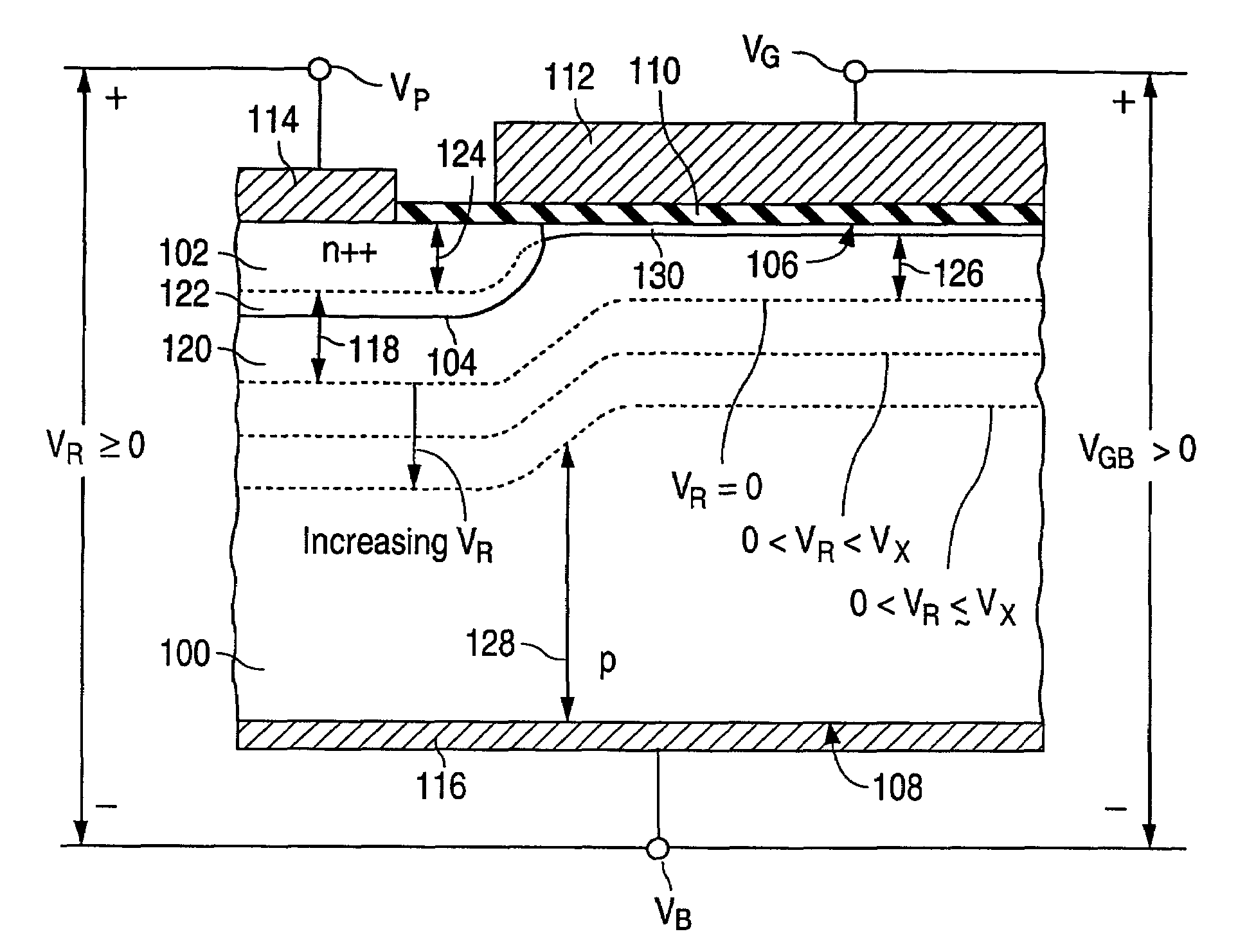
"The present invention provides a semiconductor junction varactor that can achieve a high ratio of maximum to minimum varactor capacitance. This is achieved by employing gate enhancement, which increases the maximum capacitance without needing a large amount of special processing techniques. The varactor has a simple design and can be easily fabricated using standard semiconductor manufacturing processes. The maximum-to-minimum capacitance ratio is determined by the amount of gate enhancement, which is controlled by adjusting the plate and body regions of the semiconductor body. The invention provides a method for achieving a desired maximum-to-minimum capacitance ratio by adjusting the ratio of the inversion area to the plate region area. The invention can be incorporated into a general methodology for laying out and fabricating integrated circuits. The varactor's capacitance is relatively small compared to other types of switched-capacitor varactors, making it ideal for use in small-sized integrated circuits."

Problems solved by technology

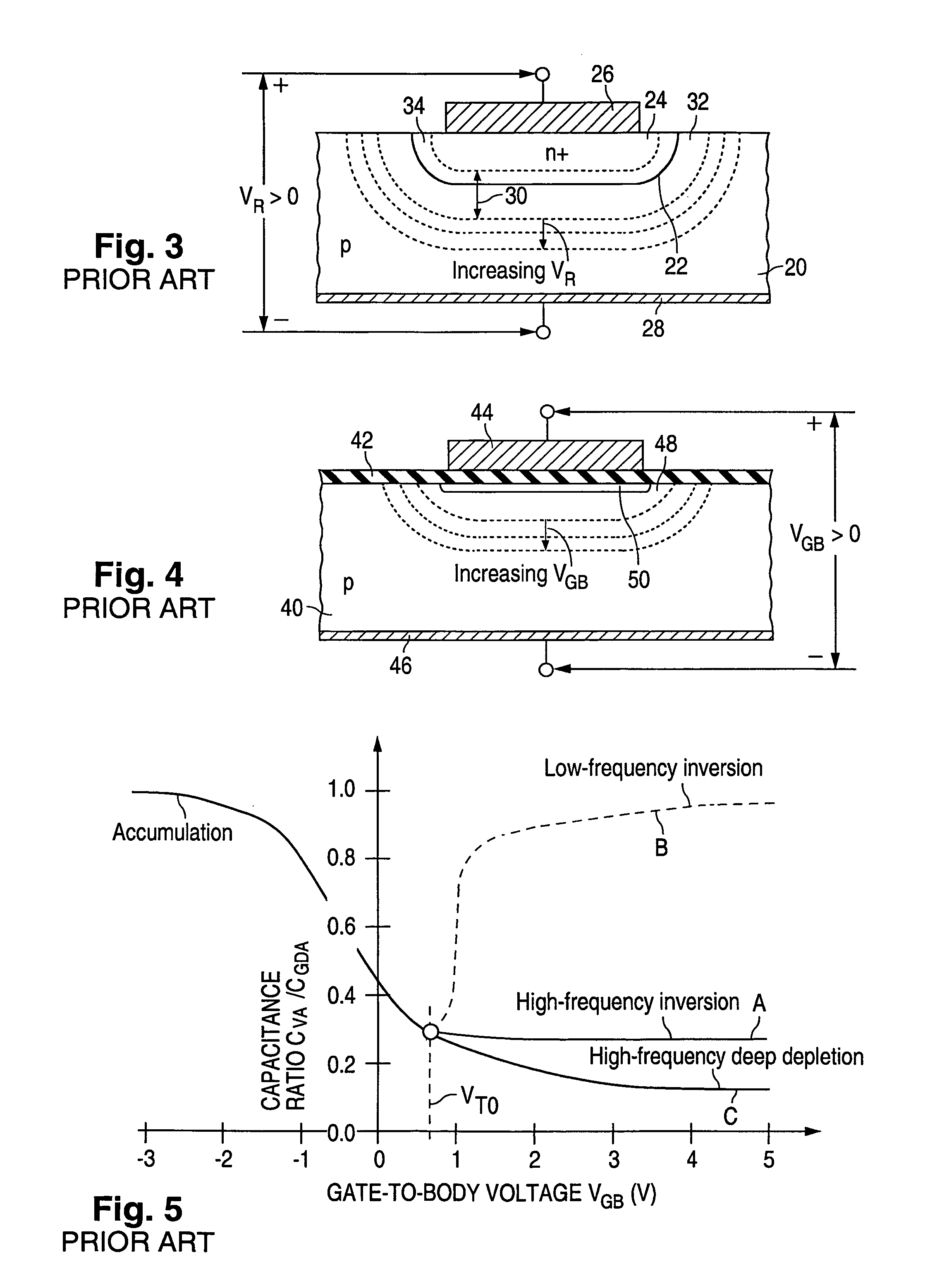
However, improving the capacitance ratio in this way necessitates an additional masked ion implantation into the varactor area and complicates the process for manufacturing an integrated circuit containing components other than the varactor.
Switched-capacitor varactors require switching control and thus are also relatively complex.

Method used


Image

  • Gate-enhanced junction varactor
  • Gate-enhanced junction varactor
  • Gate-enhanced junction varactor

Examples


Embodiment Construction

General Considerations

[0071]The term “n-channel” as used here in describing a gate-enhanced junction varactor means that the varactor has a surface charge-inversion layer (or channel) in which the charge carriers are electrons. The term “p-channel” as used here in describing a gate-enhanced junction varactor similarly means that the varactor has a surface charge-inversion layer (or channel) in which the charge carriers are holes.

[0072]An electrical signal, such as a voltage (or electrical potential), generally consists of a direct-current (“DC”) signal and / or an AC signal which varies with time at a frequency that may itself vary with time. The DC signal may vary with time. Any time variation of the DC signal is either not at a significant identifiable frequency or is at a frequency much lower than that of the AC signal. A bias signal, such as a bias voltage, is a DC signal employed to place parts of an electronic circuit, including a single circuit element, in a specified bias (e.g...


PUM


Abstract

A semiconductor junction varactor utilizes gate enhancement for enabling the varactor to achieve a high ratio of maximum capacitance to minimum capacitance.

Description

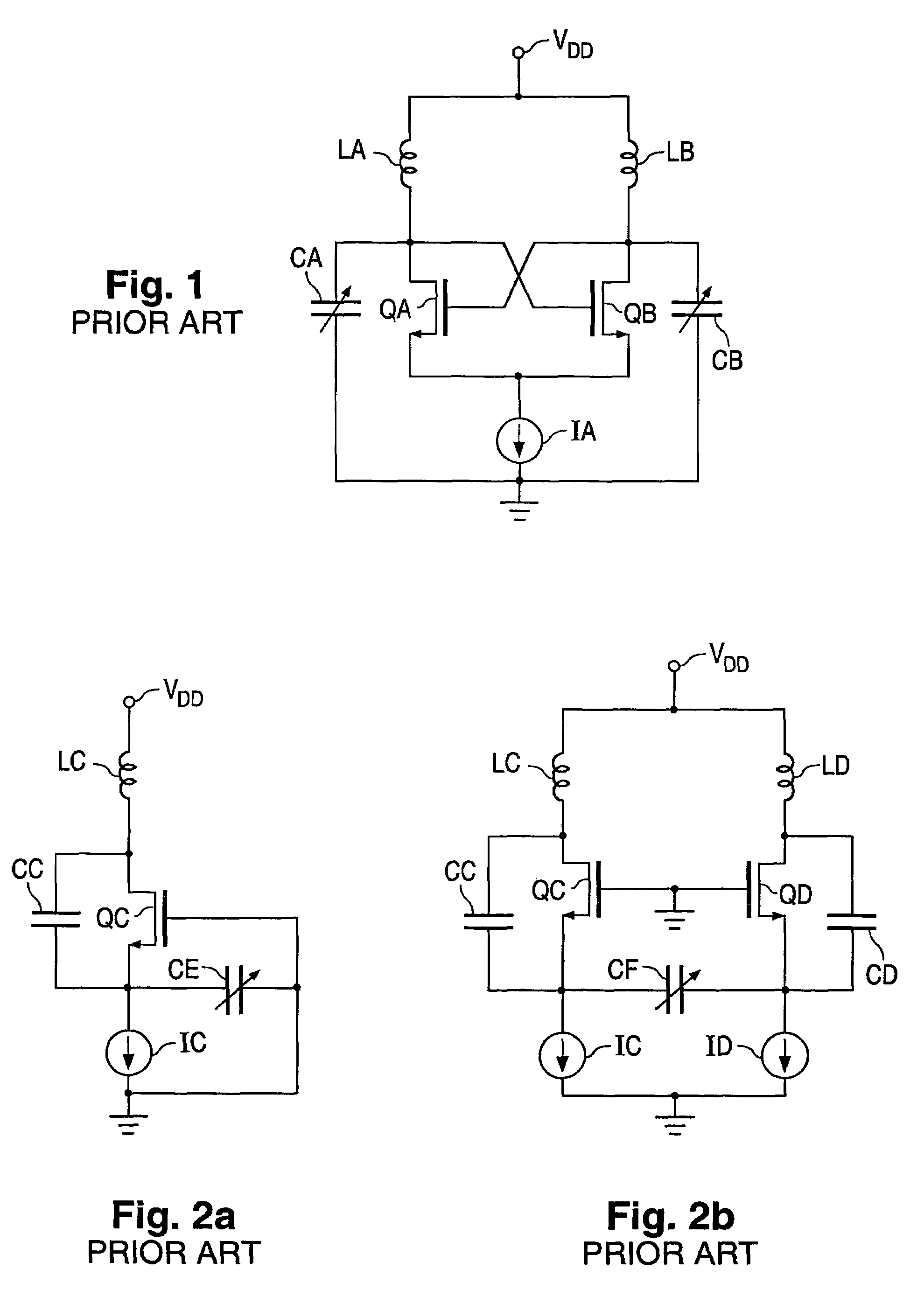
CROSS-REFERENCE TO RELATED APPLICATION[0001]This is a continuation of U.S. patent application Ser. No. 09 / 903,059, filed 10 Jul. 2001, now U.S. Pat. No. 7,235,862 B2.[0002]This invention relates to varactors. More particularly, this invention relates to varactors provided in, and / or utilized with, semiconductor integrated circuits.BACKGROUND ART[0003]A varactor is a variable capacitor, i.e., a capacitor whose capacitance can be changed as a function of one or more control signals. The term “varactor” is derived from “variable” and “reactor”, and means a device whose reactance can be varied in a controlled manner. The term “varicap”, derived from “variable” and “capacitor”, is also used to describe such a device.[0004]Varactors are employed in various parts of electronic systems. For example, varactors are utilized in voltage-controlled oscillators (“VCOs”) of wireless communications systems. A VCO generates a local oscillator signal for use in performing heterodyne frequency convers...

Claims


Application Information

Patent Timeline
Patent Type & Authority Patents(United States)
IPC IPC(8): H01L27/108H01L29/94H10B12/00H01L27/08H01L29/739H01L29/93H03B5/12
CPCH01L27/0808H01L29/7391H03B5/1243H03B5/1228H03B5/1215H01L29/93
Inventor BULUCEA, CONSTANTIN
Owner NAT SEMICON CORP
Learn More