Compensation of process and voltage variability in multi-threshold dynamic voltage scaling circuits

a voltage scaling circuit and dynamic voltage technology, applied in the field of on-chip power management technologies, can solve the problems of reducing the correlation between the variation of characteristics (such as delay) of the circuit and the closing timing requirements, and achieve the effect of reducing the effect of process variation

Inactive Publication Date: 2009-04-28
BIOLITEC PHARMA MARKETING +1
View PDF3 Cites 26 Cited by
  • Summary
  • Abstract
  • Description
  • Claims
  • Application Information

AI Technical Summary

Benefits of technology

[0007]The present invention teaches a method of minimizing variation in delay between cells in an integrated circuit comprising grouping the cells into at least two groups, wherein cells are placed in different groups if they are at least one of different VT type or in different regions of the integrated circuit, connecting cells of a first of the at least two groups of cells to a first set of at least one supply voltage, connecting cells of a second of the at least two groups of cells to a second set of at least one supply voltage; and determining a relative delay variation between the at least two groups of cells and controlling the first set of at least one supply voltage and the second set of at least one supply voltage based on the determined relative delay variation to reduce the relative delay variation between delays of the at least two groups of cells.
[0009]An aspect of another embodiment of the present invention provides for the apparatus and method in which these supply and body bias voltage controls can be combined such that the signals do not overlap. For example, adaptive body bias can be used to reduce the effects of process variation in a region-based technique while supply voltages can individually tune the different device types, as described in more detail in the following section.

Problems solved by technology

These differences can cause difficulties in closing timing requirements for systems employing voltage scaling, where the worst-case critical path may depend on the specific supply voltage used.
This delay variability is compounded by process variability which is becoming more significant as device dimensions shrink, and also affects the various threshold and gate length devices differently, decreasing the correlation between the variation of characteristics (such as delay) of those circuits.

Method used


Image

  • Compensation of process and voltage variability in multi-threshold dynamic voltage scaling circuits
  • Compensation of process and voltage variability in multi-threshold dynamic voltage scaling circuits
  • Compensation of process and voltage variability in multi-threshold dynamic voltage scaling circuits

Examples


Embodiment Construction

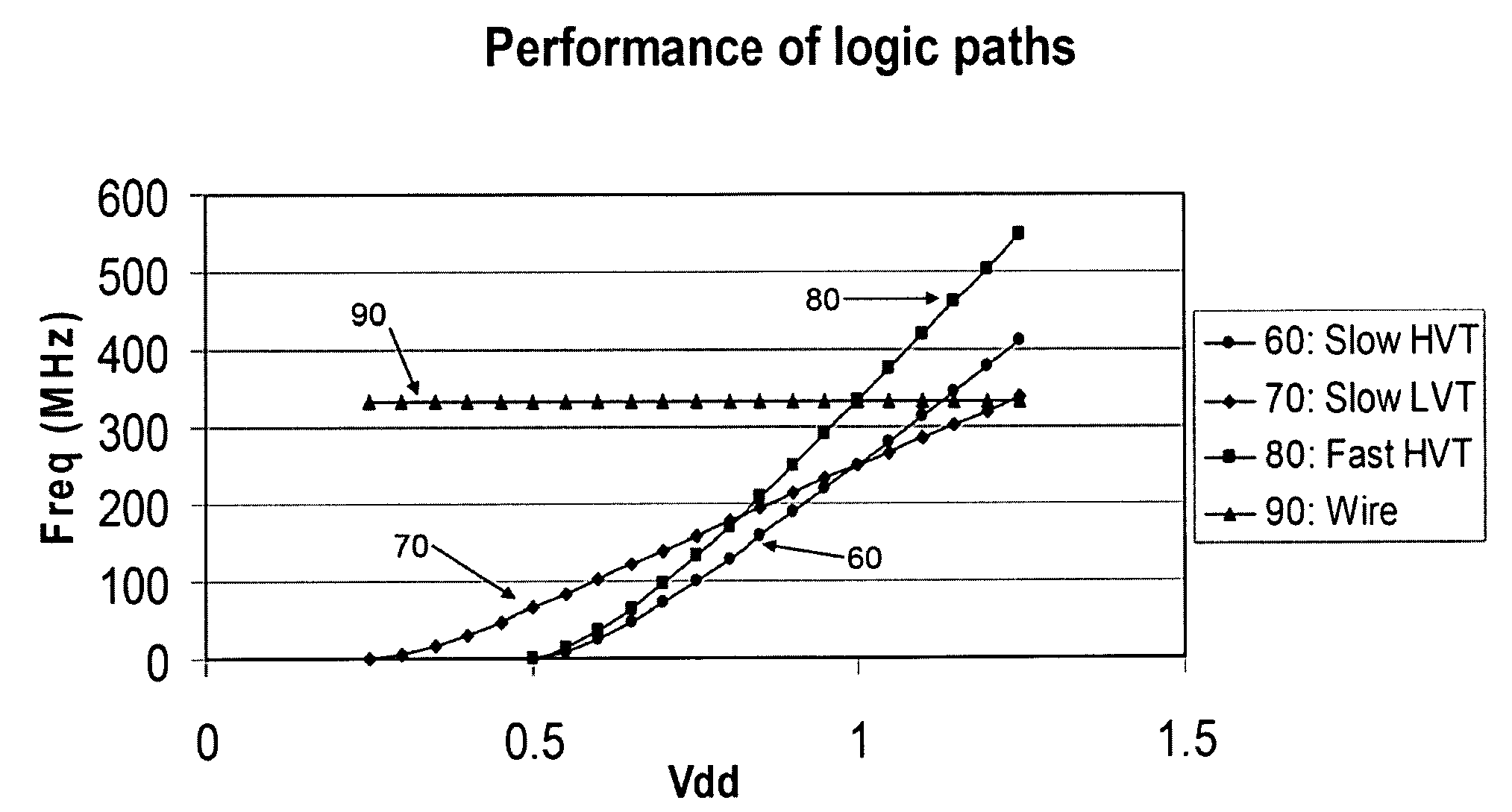
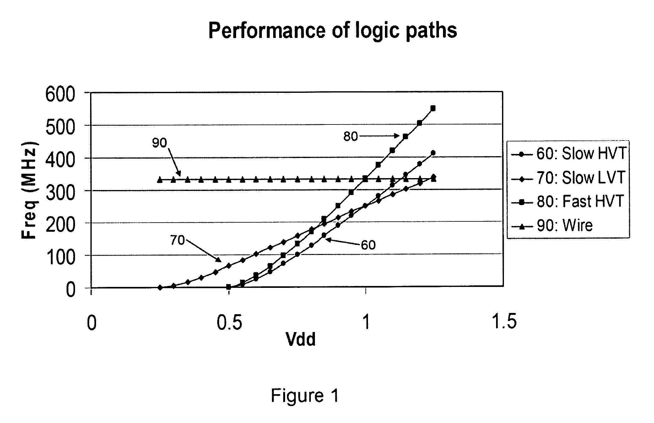
[0016]In the present invention, threshold voltage VT is conventionally defined as representing the gate to source voltage (VGS) of a transistor at which the transistor “turns on” (i.e., at a point which significant drain to source current can begin flow. It is a common occurrence that lower levels of leakage current can flow at voltages where the gate to source voltage is less than or equal to the threshold voltage (i.e. at VGS≦VT).

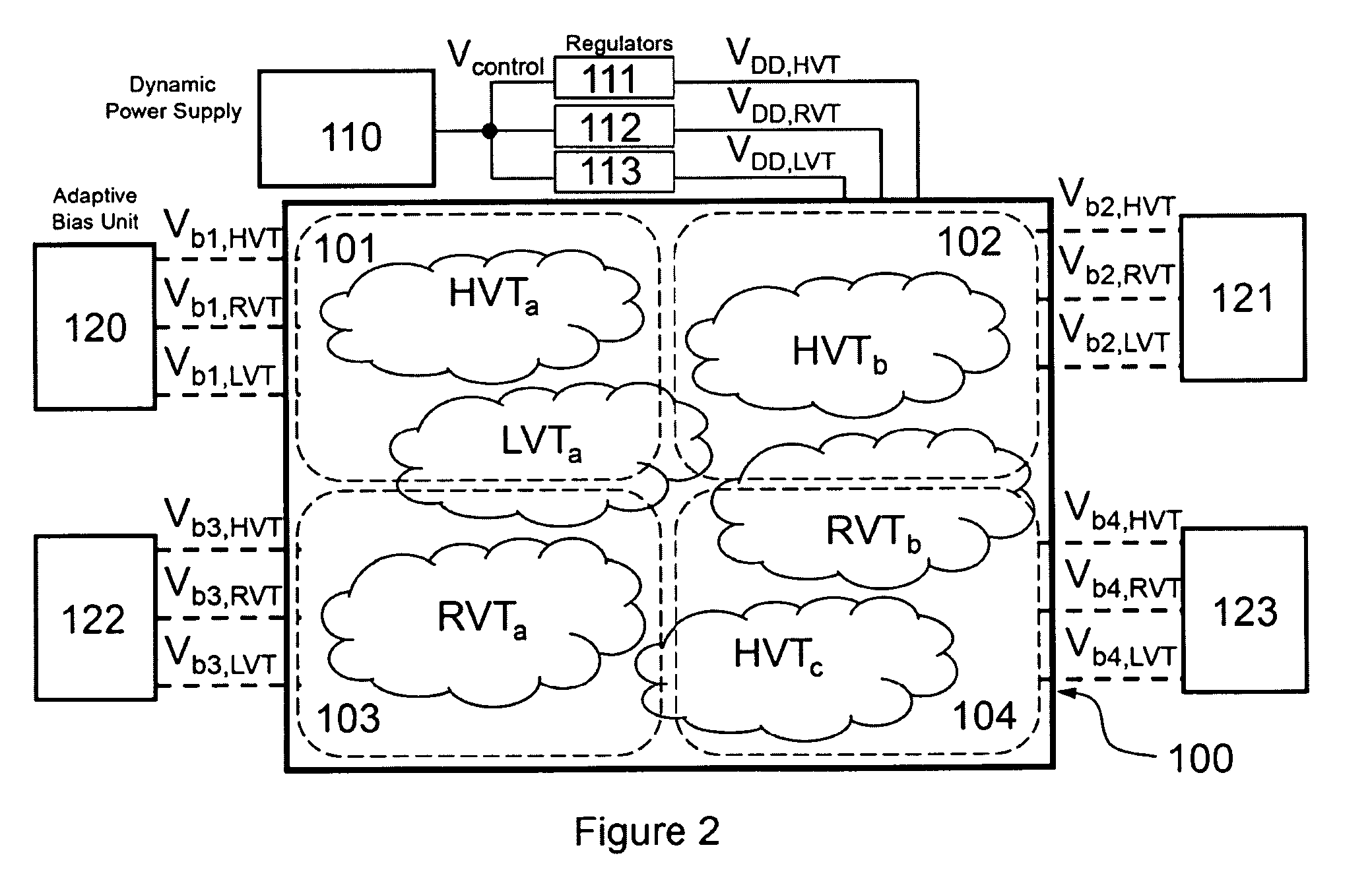
[0017]Silicon On Insulator (hereinafter, “SOI”) is a method of constructing an integrated circuit in which the “body” of the transistor, (i.e. the region in which the conduction channel forms) is built on top of an insulating layer. This is generally in contrast to “bulk”, where the transistor bodies are built in “wells” that are isolated from the substrate, or bulk, of the IC by a reverse-biased N-P junction. The relevance to the current invention is that one must apply a voltage to the well region (in “bulk”) to maintain this reverse bias that isolates ...


PUM


Abstract

This invention relates to adaptively compensating for variations in integrated chip circuitry due to delays caused by multiple thresholds. The multi-threshold adaptive dynamic scaling system disclosed compensates for normal on-chip variations which affect system process and voltage variability, as well as overall performance. This system regulates a voltage control and provides high voltage thresholds, regular voltage thresholds, and low voltage thresholds to compensate for threshold voltage variations.

Description

CROSS REFERENCE TO RELATED APPLICATIONS[0001]There are no cross-references related to this application.FIELD OF THE INVENTION[0002]The present invention relates to on-chip power management technologies. The present invention more particularly relates to multi-threshold adaptive dynamic scaling systems used to compensate for nonnal on-chip variations which affect system perfomiance. Relevant potential applications for the present invention include CMOS circuits, integrated chip manufacture, microprocessors, portable computers, portable handheld devices, portable media player, digital cameras, low power electronics, and other battery powered electronics.BACKGROUND OF THE INVENTION[0003]The use of multiple-threshold and multiple gate length devices on a chip has become popular in IC design for handling the trade-off between speed and leakage power. These techniques are now being combined with other low-power techniques such as voltage scaling for further reducing system power.[0004]Vol...

Claims


Application Information

Patent Timeline
Patent Type & Authority Patents(United States)
IPC IPC(8): H01L25/00
CPCG06F1/3296G06F1/3203G06F17/5072G06F1/3287G06F2217/78G06F2217/84Y02B60/1282H01L27/0207Y02B60/1285Y02B60/1278G06F30/392G06F2119/06G06F2119/12Y02D10/00
Inventor OGILVIE, CLARENCE ROSSERWOLPERT, DAVID SOLOMONHATHAWAY, DAVID JAMES
Owner BIOLITEC PHARMA MARKETING
Why Eureka
Try Eureka