Probe unit substrate

a technology of probe unit and substrate, applied in the direction of printed circuit, printed circuit structure association, instruments, etc., can solve the problem of complex manufacturing process, and achieve the effect of alleviating surface irregularities of multi-layer wiring division

Active Publication Date: 2009-03-17
NIHON MICRONICS
View PDF5 Cites 2 Cited by
  • Summary
  • Abstract
  • Description
  • Claims
  • Application Information

AI Technical Summary

Benefits of technology

[0015]The probe unit substrate according the present invention has an advantage that the surface irregularity of the multilayer wiring division is alleviated so that the probe mounting pads on its surface neither undulate nor slope because of the formation of the flatness improvement rings or the planarization patterns as described above. Therefore, there is no variation in heights of the tips of the probes that are fixed to a number of the probe mounting pads respectively.

Problems solved by technology

However, if the distance d is reduced, another problem occurs as described below.
According to the above-described technique disclosed in the first publication, the surface irregularity of the multilayer wiring substrate is reduced, but the manufacturing process will be complicated to form “a covering resin layer having through-holes”.

Method used


Image

  • Probe unit substrate
  • Probe unit substrate
  • Probe unit substrate

Examples


first embodiment

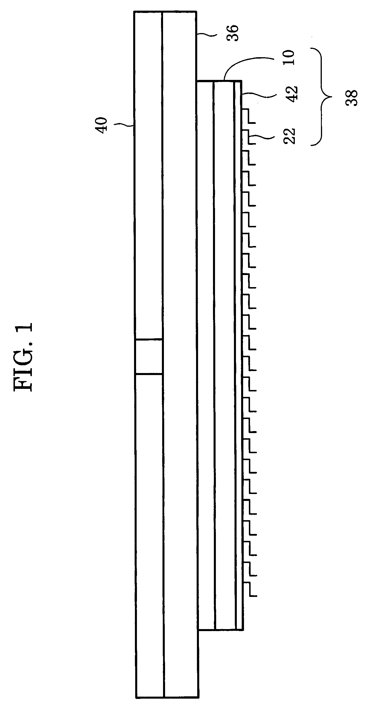
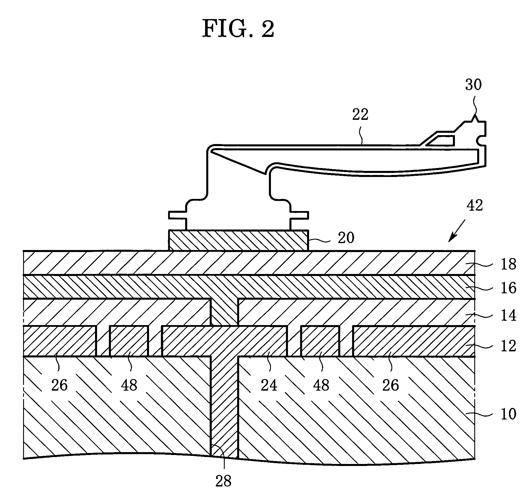
[0030]FIG. 2 is a side sectional view of a part of the probe unit substrate according to the present invention. On the ceramic substrate 10 is formed the multilayer wiring division 42, on which the micro cantilever type probes 22 are fixed. The ceramic substrate 10 corresponds to the electrical insulating substrate in the present invention. The multilayer wiring division 42 consists of the first conductor layer 12, the first insulating layer 14, the second conductor layer 16 and the second insulating layer 18. The first conductor layer 12 includes through-hole junction pads 24, flatness improvement rings 48 that surround the through-hole junction pads 24, and a grounding region 26 that further surrounds the flatness improvement rings 48. The ceramic substrate 10 is formed with through-holes 28. Conductors buried inside the through-holes 28 are connected with the through-hole junction pads 24 respectively. The through-hole junction pad 24 is formed for the purpose of absorbing a posi...

second embodiment

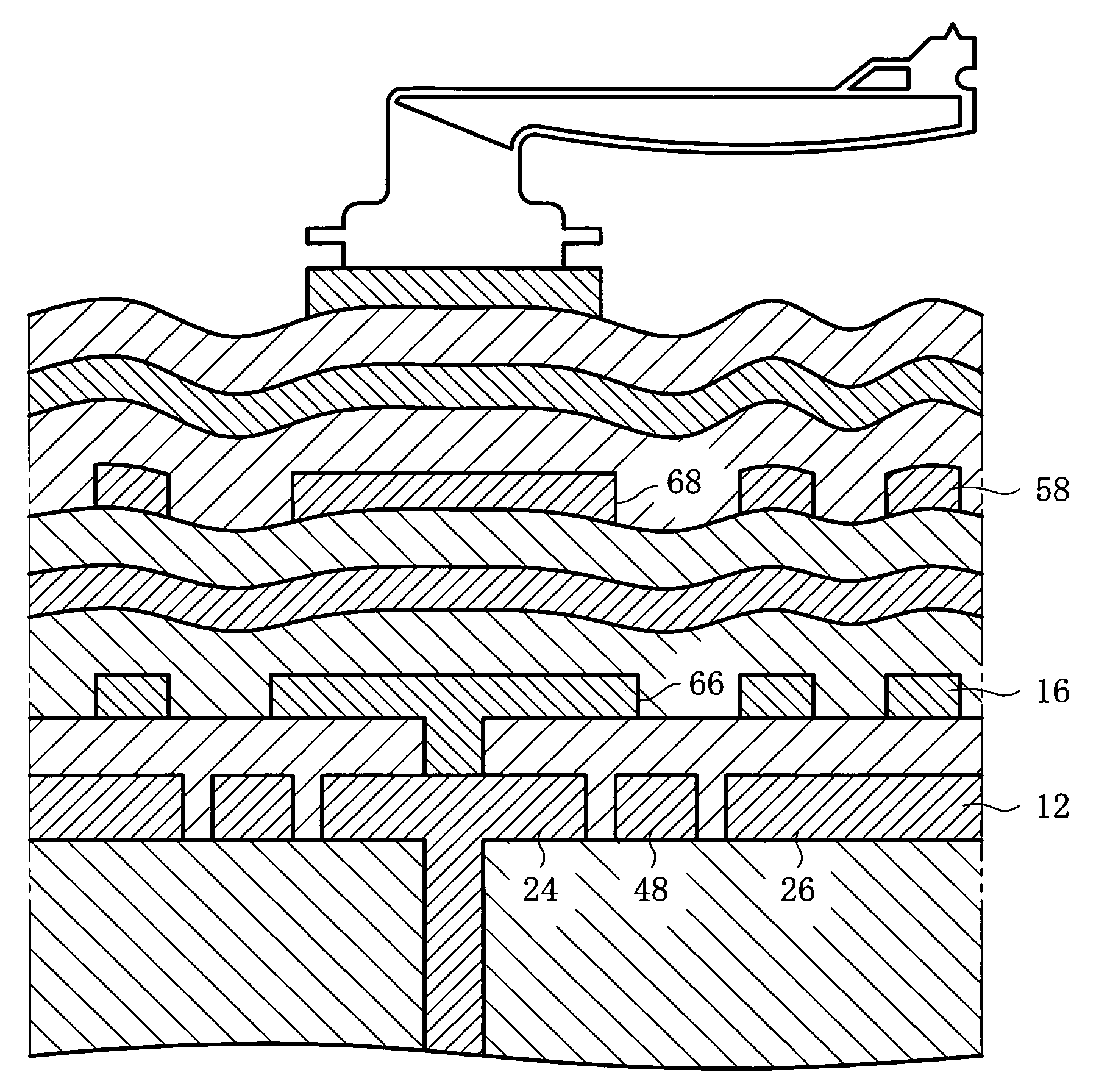
[0033]FIG. 4 is a side sectional view of a part of the probe unit substrate according to the present invention. This embodiment has no above-described flatness improvement ring but planarization patterns. The multilayer wiring division 42 in this embodiment consists of the first conductor layer 12, the first insulating layer 14, the second conductor layer 16, the second insulating layer 18, the third conductor layer 54, the third insulating layer 56, the fourth conductor layer 58, the fourth insulating layer 60, the fifth conductor layer 62, and the fifth insulating layer 64. On the surface of the fifth insulating layer 64 are formed a number of probe mounting pads 20.

[0034]The first conductor layer 12 includes the through-hole junction pads 24 and the grounding region 26 that surrounds the through-hole junction pads 24, but has no flatness improvement ring. The second conductor layer 16, the third conductor layer 54 and the fourth conductor layer 58 are wiring layers. On the other ...


PUM


Abstract

A ceramic substrate has, on its surface, a multilayer wiring division, on which micro cantilever type probes are fixed. The multilayer wiring division has the first conductor layer, which includes through-hole junction pads, flatness improvement rings surrounding the through-hole junction pads and a grounding region further surrounding the flatness improvement rings. Since the flatness improvement rings are located around the through-hole junction pads, the surface of the first insulating layer, which is located above the first conductor layer, is free from severe undulation even near the through-hole junction pads. Accordingly, the multilayer wiring division has less irregularity in shape as a whole, and thus the probe mounting pads on the surface of the second insulating layer do not slope but keep almost horizontal. The probe unit substrate according to the invention has an advantage of less surface undulation and having non-sloping probe mounting pads without using a complicated manufacturing process.

Description

BACKGROUND OF THE INVENTION[0001]The present invention relates to a probe unit substrate having a feature of planarization or leveling of probe mounting pads.[0002]In this specification, the phrase “probe unit” signifies a unit having plural probes for testing electronic parts or electrical parts, and thus it corresponds to, for example, a probe card used for testing an electrical circuit on a semiconductor wafer or a probe unit used for testing a liquid crystal display. Further, the phrase “probe unit substrate” signifies a substrate for the probe unit, which has an internal wiring and is possible to support plural probes.[0003]FIG. 11 is an enlarged sectional view illustrating a part of a conventional probe unit substrate. A ceramic substrate 10 has a surface, on which the first conductor layer 12 is formed in a predetermined pattern. Above the first conductor layer 12 are formed the first insulating layer 14, the second conductor layer 16, and the second insulating layer 18 in or...

Claims


Application Information

Patent Timeline
Patent Type & Authority Patents(United States)
IPC IPC(8): G01R31/02
CPCG01R1/06727G01R1/0735
Inventor FUKAMI, YOSHIYUKI
Owner NIHON MICRONICS
Why Eureka
Try Eureka