Printed board and manufacturing method thereof
a printing board and manufacturing method technology, applied in the field of printed boards, can solve the problems of high heat generation of electronic components, such as transistors and integrated circuits, packaged on printed boards, and achieve the effects of excellent heat generation characteristic, easy manufacturing, and excellent heat radiating characteristi
- Summary
- Abstract
- Description
- Claims
- Application Information
AI Technical Summary
Benefits of technology
Problems solved by technology
Method used
Image
Examples
first embodiment
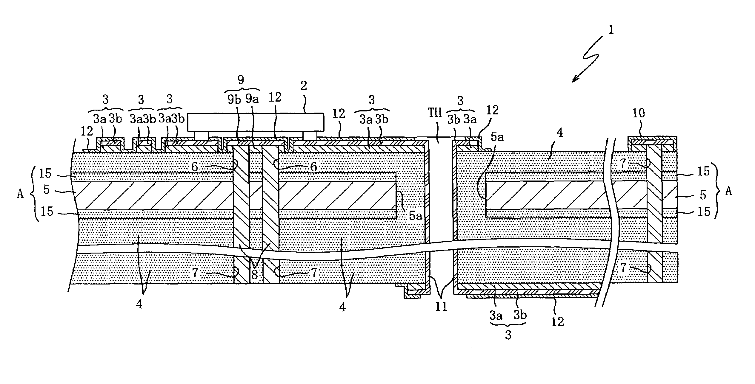
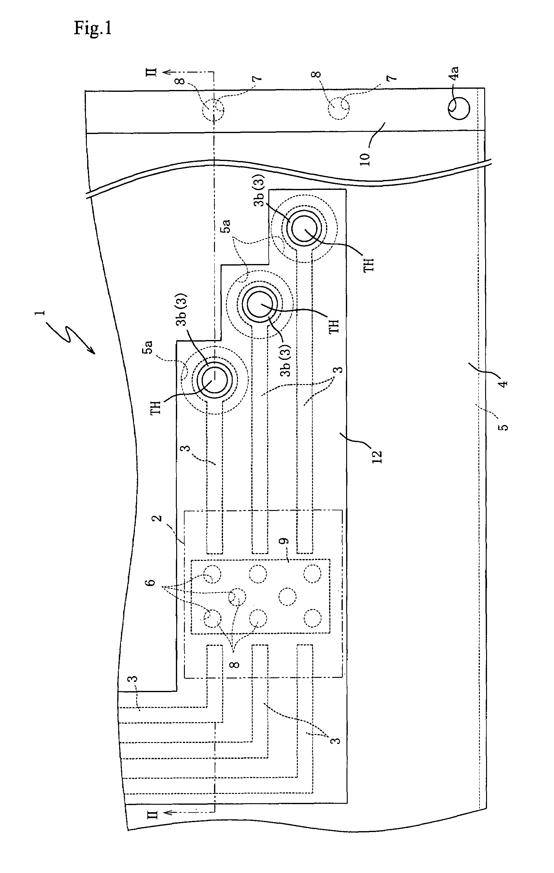
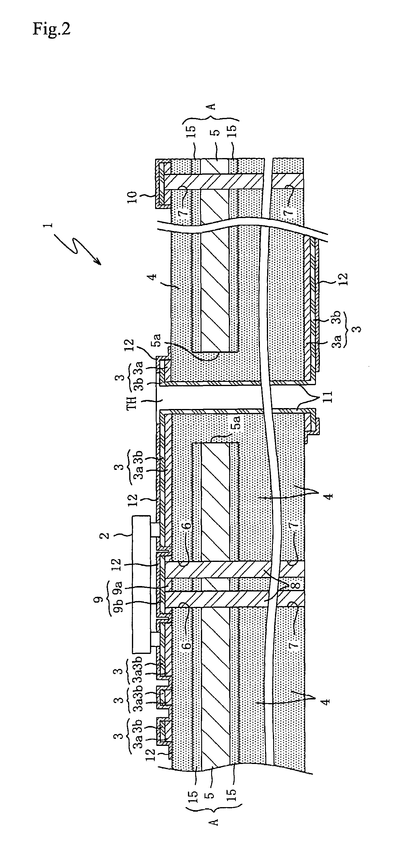
[0079]Preferred embodiments of the present invention will be described below with reference to the accompanying drawings. FIG. 1 is a top view of a printed board 1 according to the present invention. FIG. 2 is a sectional side view taken along line II-II of FIG. 1. In FIGS. 1 and 2, the printed board 1 is partially omitted. In FIG. 1, an electronic component 2 is not shown and its imaginary outline is shown using a chain double-dashed line.
[0080]The printed board 1 is, for example, a board included in an electronic device such as an engine control unit (ECU). It principally includes a plurality of electronic components 2 packaged on an upper surface thereof (toward a viewer from paper surface of FIG. 1, upper side in FIG. 2), a conductive pattern 3 for coupling these electronic components 2, an insulating board 4 on whose at least one surface (upper surface of the insulating board 4 in FIG. 2) the conductive pattern 3 is formed, and a carbon sheet 5 provided inside the insulating bo...
second embodiment
[0149]Similarly in the carbon sheet 50 used in the second embodiment, the carbon containing material 50a filling the network knitted from the copper wire 50b may be made of only carbon or a mixture of carbon and other materials.
[0150]Further, in the carbon sheet 50 used in the second embodiment, the network knitted from the copper wire 50b is filled with the carbon containing material 50a. However, the member forming the network is not limited to the copper wire 50b. As a matter of course, it can be presumed that the copper wire 50b can be replaced with a material having heat conductivity. For example, a metal wire such as a silver wire may be used instead of the copper wire 50b. Further, the mesh form of the network is not limited to the knit form shown in FIG. 6. As a matter of course, it can be presumed that the network can take other mesh forms.
[0151]Further, as the method for manufacturing the printed board 1 according to the above-mentioned first embodiment, the method for man...
PUM
 Abstract
Description
Claims
Application Information
 - R&D
- Intellectual Property
- Life Sciences
- Materials
- Tech Scout
- Unparalleled Data Quality
- Higher Quality Content
- 60% Fewer Hallucinations
Browse by: Latest US Patents, China's latest patents, Technical Efficacy Thesaurus, Application Domain, Technology Topic, Popular Technical Reports.
© 2025 PatSnap. All rights reserved.Legal|Privacy policy|Modern Slavery Act Transparency Statement|Sitemap|About US| Contact US: help@patsnap.com


