Incident light angle detector for light sensitive integrated circuit
a detector and integrated circuit technology, applied in the direction of semiconductor/solid-state device testing/measurement, vacuum evaporation coating, coating, etc., can solve the problems of photodiode design and fabrication constraints, the least one aspect of a combination of features including fabrication cost, size, measurement resolution of disclosed detector configurations is undesirable for many applications, etc., to achieve the effect of reducing potential unwanted diffraction effects
- Summary
- Abstract
- Description
- Claims
- Application Information
AI Technical Summary
Benefits of technology
Problems solved by technology
Method used
Image
Examples
first embodiment
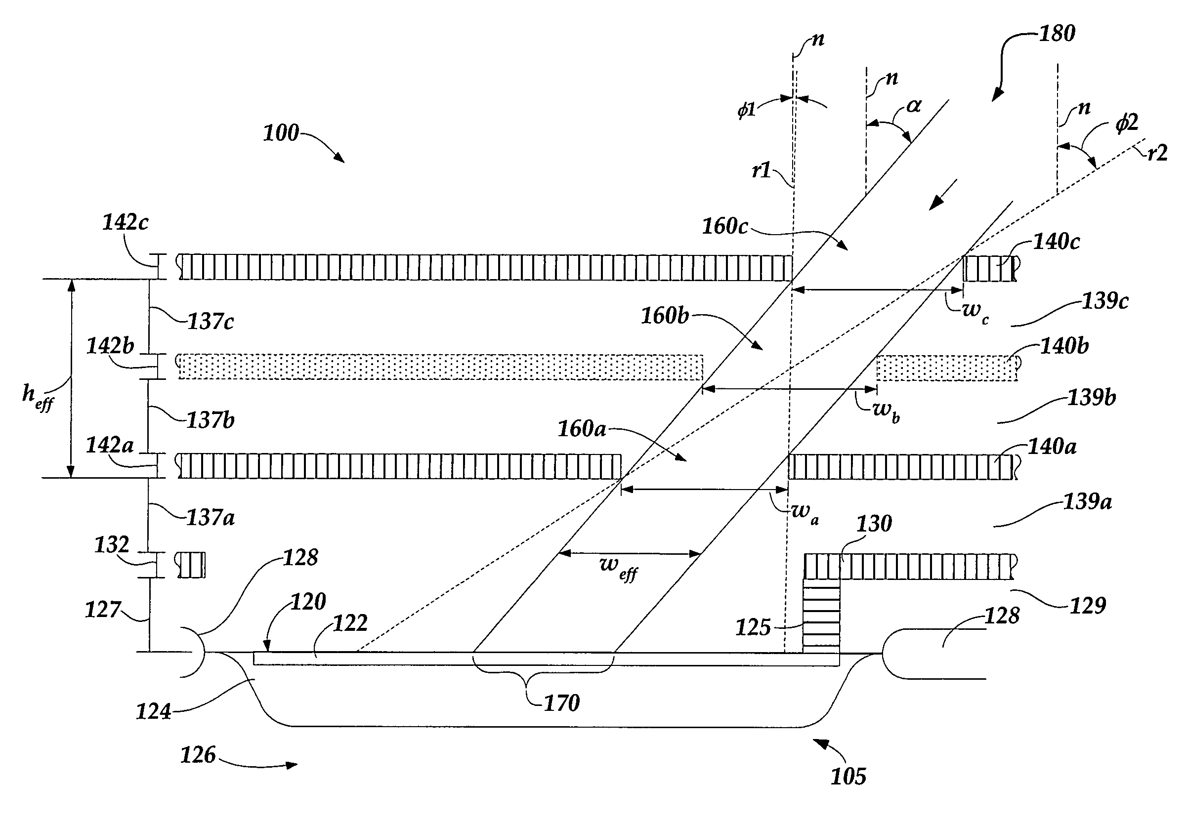
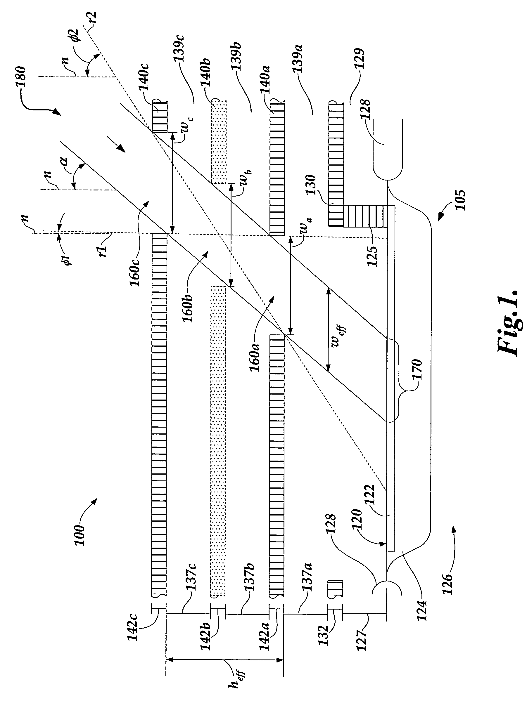
[0022]FIG. 1 is a diagram of a detector configuration 100 with an angled interlayer optical path 180 directed toward a photodetector 105 for sensing radiation at an angle of incidence corresponding to an angle α. The detector configuration 100 may be one of a plurality of similar configurations included a photodetector IC. The function of the detector configuration 100 may be an auxiliary function of the photodetector IC (e.g., an imaging array IC) as described in greater detail below. Each reference line n shown in FIG. 1 represents a vector normal to a nominal surface plane of the photodetector IC. While a photodiode type photodetector is illustrated, it will be appreciated that any light sensitive element could also be utilized, such as a photogate, photo-transister, etc. The term light, as used herein, is not restricted to visible radiation. As shown in FIG. 1, the photodetector 105 includes a surface 120, an N+ diffusion layer 122, a P well 124, a P substrate 126 and a field ox...
second embodiment
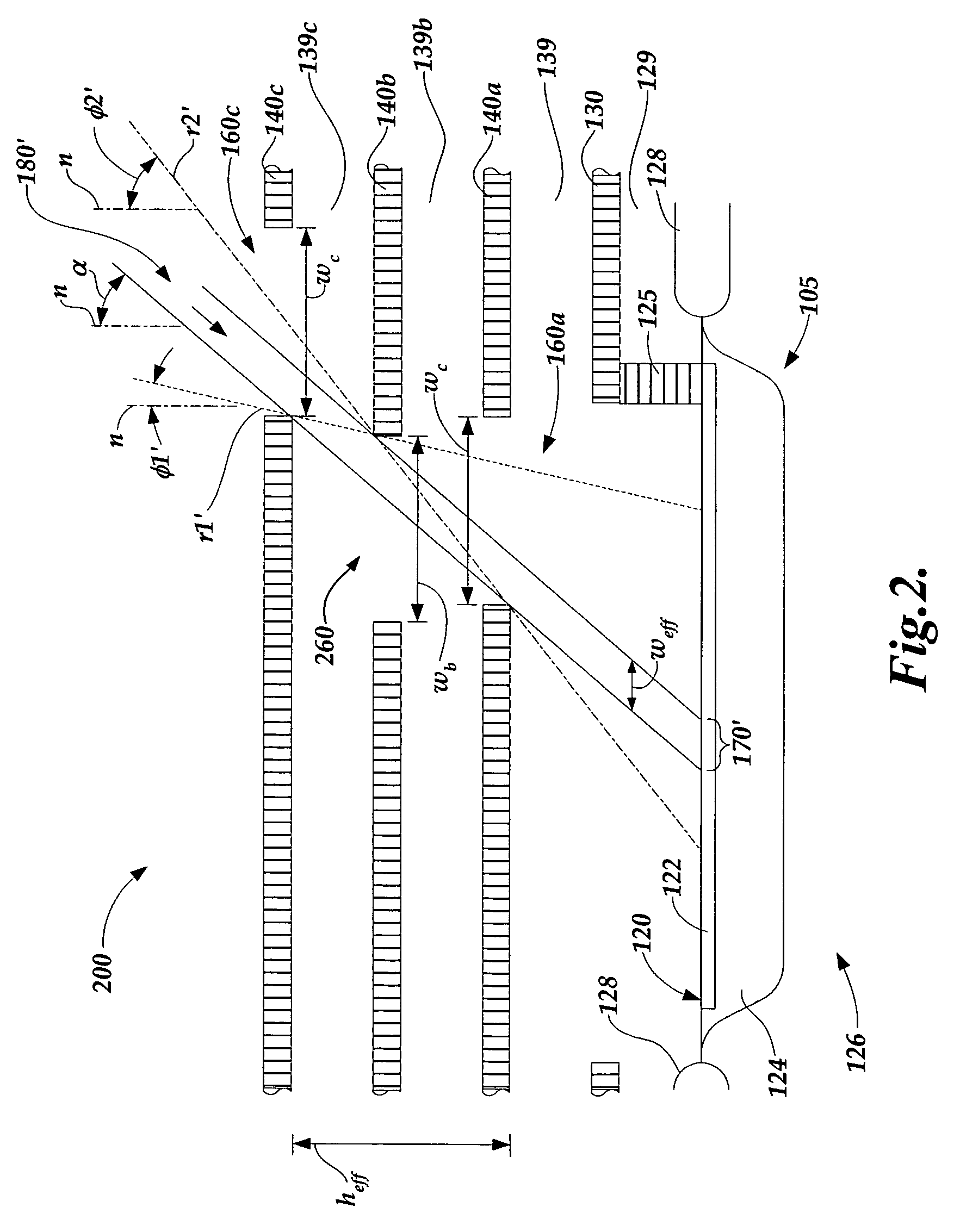
[0030]FIG. 2 is a diagram of a detector configuration 200 with an angled interlayer optical path 180′ directed toward a photodetector 105 for sensing radiation at an angle of incidence corresponding to an angle α. The illustrated components of the detector configuration 200 are similar to those of FIG. 1, except as otherwise described below. Each of the metal layers 130, 140a, 140b′ and 140c and insulating layers 129, 139a, 139b, 139c, may be similarly fabricated and have similar thicknesses.
[0031]In contrast to the detector configuration 100, in the embodiment shown in FIG. 2, the “interior” metal layer 140b′ provides an important function in defining the angled interlayer optical path 180′, and is not optional in the vicinity of the photodetector 105. It should be appreciated that when the thicknesses and materials of each metal layer and each insulating layer are advantageously the standard thicknesses and materials used to fabricate other structures on the photodetector IC, that...
PUM
| Property | Measurement | Unit |
|---|---|---|
| thicknesses | aaaaa | aaaaa |
| thicknesses | aaaaa | aaaaa |
| azimuthal angle | aaaaa | aaaaa |
Abstract
Description
Claims
Application Information
 - R&D
- Intellectual Property
- Life Sciences
- Materials
- Tech Scout
- Unparalleled Data Quality
- Higher Quality Content
- 60% Fewer Hallucinations
Browse by: Latest US Patents, China's latest patents, Technical Efficacy Thesaurus, Application Domain, Technology Topic, Popular Technical Reports.
© 2025 PatSnap. All rights reserved.Legal|Privacy policy|Modern Slavery Act Transparency Statement|Sitemap|About US| Contact US: help@patsnap.com


