Organic conductive material and conductive varnish
a technology of organic conductive materials and conductive varnish, which is applied in the direction of electrically conductive paints, non-metal conductors, conductors, etc., can solve the problems of product solubility decline, unsolved problem of solubility, and affect the solubility of solvents
- Summary
- Abstract
- Description
- Claims
- Application Information
AI Technical Summary
Benefits of technology
Problems solved by technology
Method used
Image
Examples
example 1
[Preparation of Phenyltetraaniline Varnish]
[0075]
[0076]In 2 liters of toluene was dissolved 12.977 g of p-phenylenediamine. In the resulting solution was dissolved 245.05 g of tetra-n-butoxy titanium (which is a dehydration condensing agent) at 70° C. over 30 minutes. To the solution was added 53.346 g of p-hydroxydiphenylamine, and the solution was heated at 100° C. for 24 hours under a nitrogen atmosphere. After the reaction was complete, the reaction mixture was filtered and separated solids were washed sequentially with toluene and ether and finally dried. Thus there were obtained silvery crystals. The crystals, together with 0.2 mol of hydrazine monohydrate, were dissolved in as much dioxane as 25 times the weight of the crystals, by heating with refluxing, with the atmosphere in the reaction system replaced by nitrogen. To the resulting solution was added as much toluene as 25 times the weight of the crystals, so that the solution was suspended in toluene. The resulting suspen...
example 2
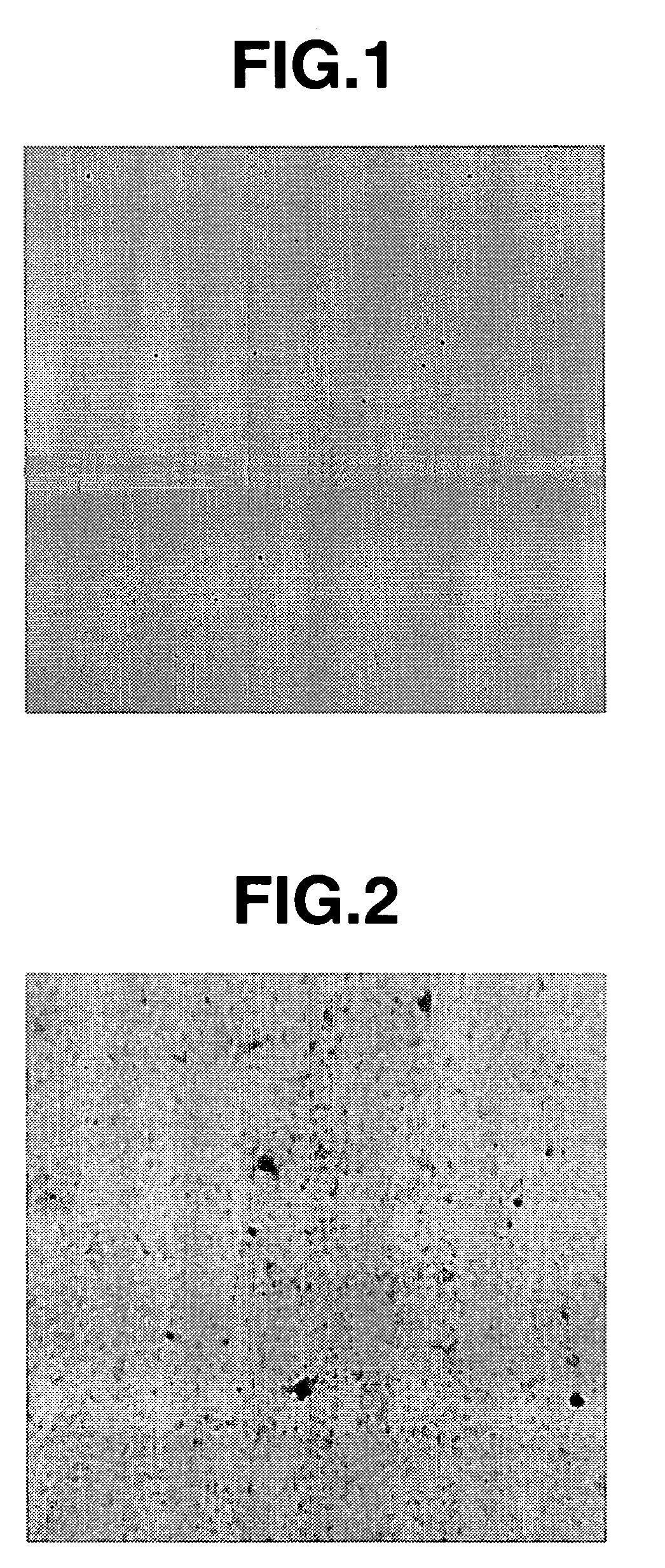
[0084]The conductive varnish designated as Run No. 4 in Table 1 was applied by spin coating to an ITO glass substrate which had undergone ozone cleaning for 40 minutes. The coated substrate was baked at 180° C. for 2 hours on a hot plate. Thus there was obtained a conductive thin film, 40 nm thick. The conductive thin film was observed under a confocal laser microscope, whose microphotograph is shown in FIG. 1.
example 3
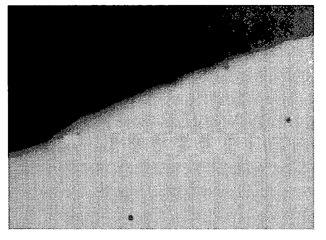
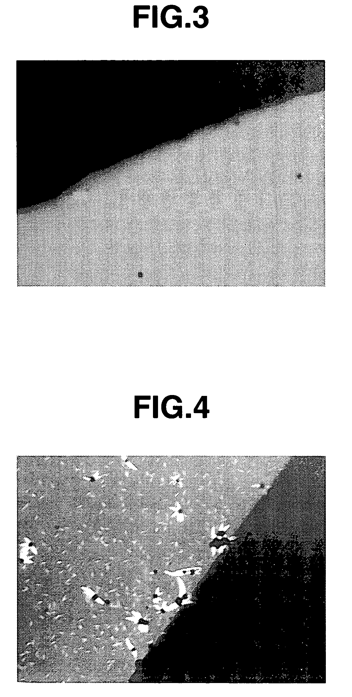
[0086]The conductive varnish designated as Run No. 4 in Table 1 was applied by spin coating to an ITO glass substrate which had undergone ozone cleaning for 40 minutes. The coated substrate was baked at 180° C. for 2 hours on a hot plate so as to form a hole injection layer (20 nm thick). The substrate was placed in a vacuum deposition apparatus, and vapor deposition was performed to form four layers sequentially as follows.[0087](α-naphthyldiphenylamine)dimer (α-NPD), 40 nm thick.[0088]tris(8-quinolinolate aluminum (III)) (Alq3), 60 nm thick.[0089]LiF, 0.5 nm thick.[0090]Al, 100 nm thick.
Vapor deposition for each layer was carried out at a pressure no higher than 8×10⁻⁴ Pa. The rate of deposition was 0.3-0.4 nm / s (except for the LiF layer). The rate of deposition for the LiF layer was 0.02-0.04 nm / s. The substrate was transferred in a vacuum from one step to another. The thus obtained organic electroluminescence element has the characteristic properties as shown in Table 3. The pho...
PUM
| Property | Measurement | Unit |
|---|---|---|
| carbon number | aaaaa | aaaaa |
| carbon number | aaaaa | aaaaa |
| temperature | aaaaa | aaaaa |
Abstract
Description
Claims
Application Information
 - R&D
- Intellectual Property
- Life Sciences
- Materials
- Tech Scout
- Unparalleled Data Quality
- Higher Quality Content
- 60% Fewer Hallucinations
Browse by: Latest US Patents, China's latest patents, Technical Efficacy Thesaurus, Application Domain, Technology Topic, Popular Technical Reports.
© 2025 PatSnap. All rights reserved.Legal|Privacy policy|Modern Slavery Act Transparency Statement|Sitemap|About US| Contact US: help@patsnap.com


