Methods and systems for analyzing a specimen using atomic force microscopy profiling in combination with an optical technique
- Summary
- Abstract
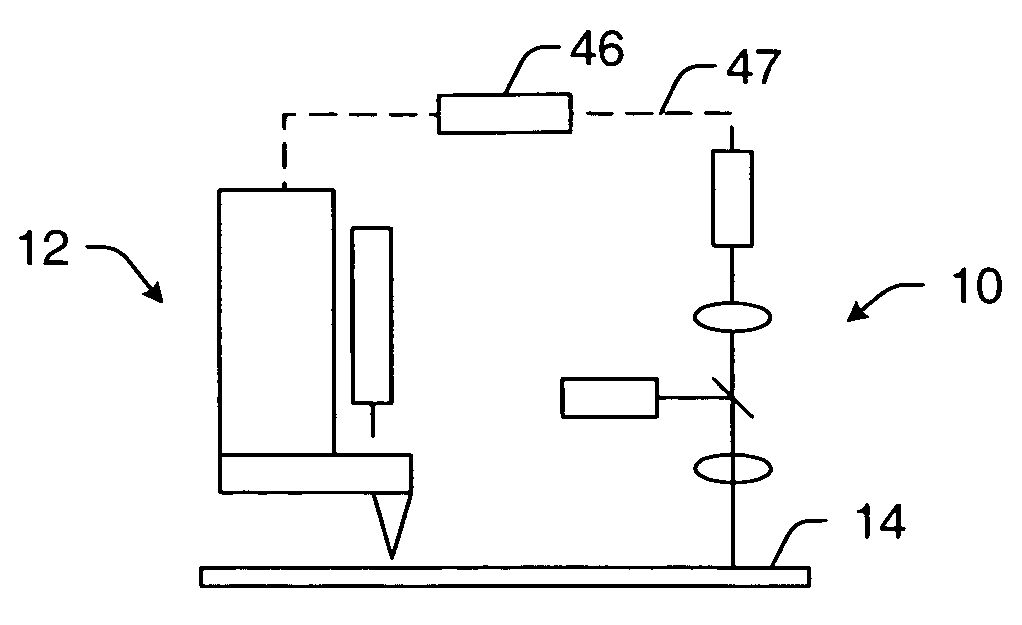
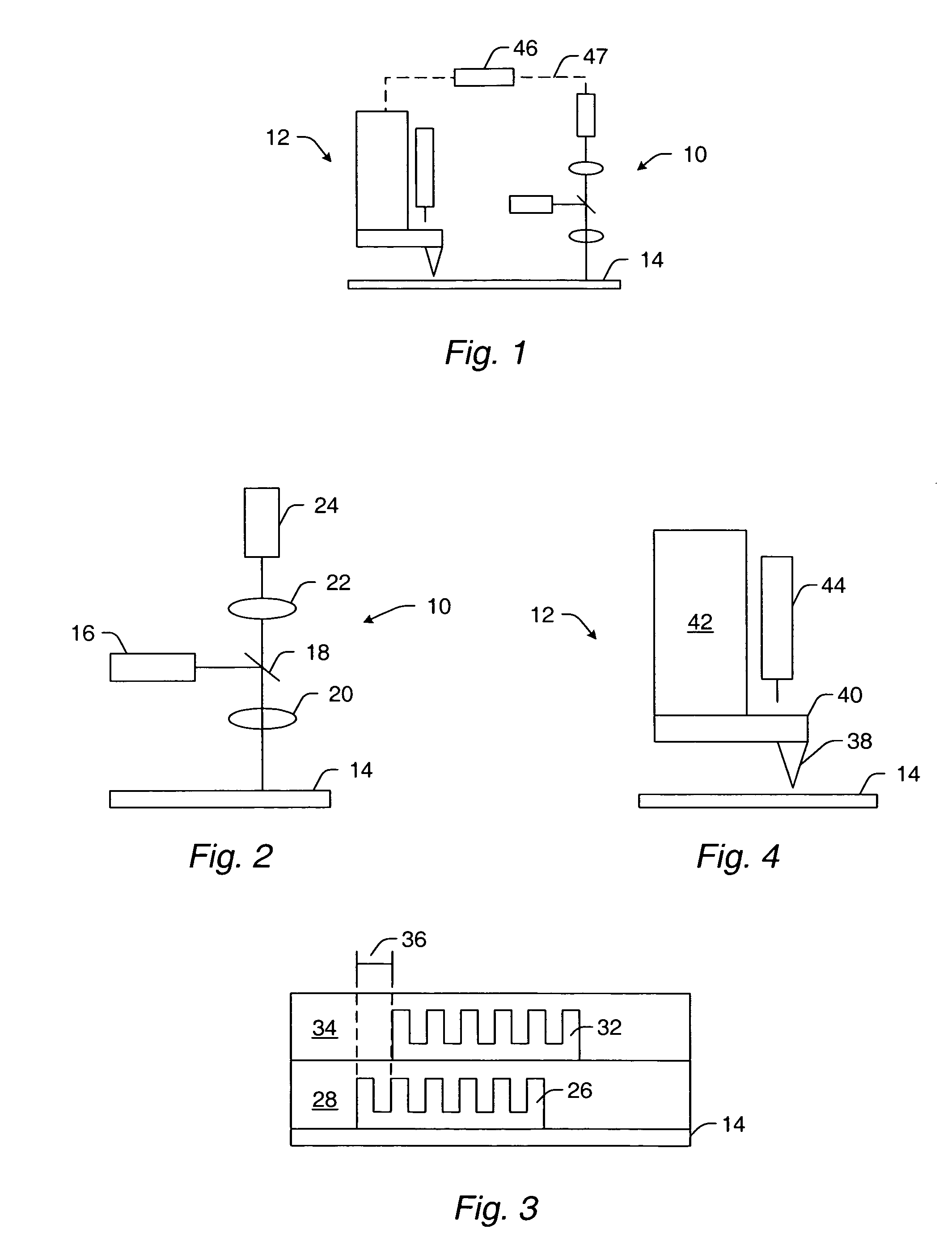
- Description
- Claims
- Application Information
AI Technical Summary
Problems solved by technology
Method used
Image

Examples
Embodiment Construction
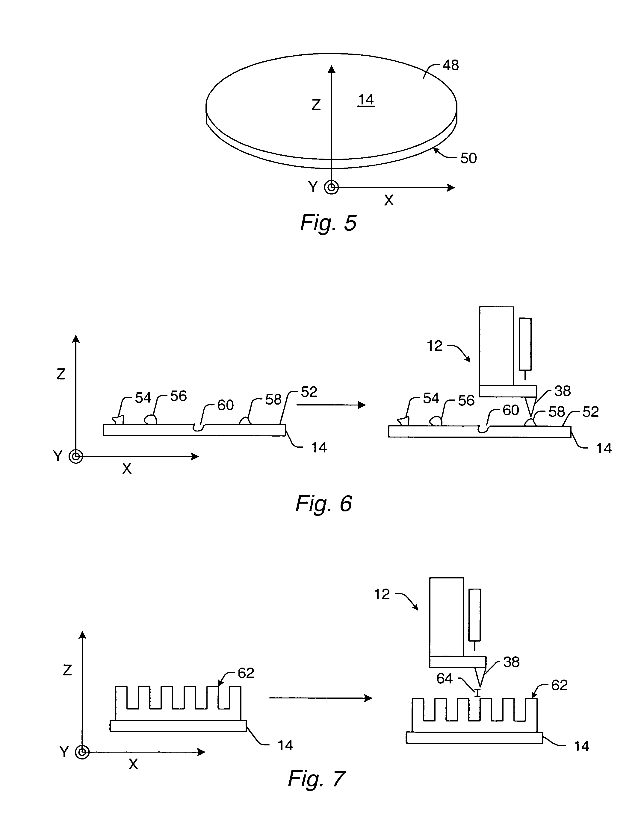
[0040]As used herein, the term “specimen” refers to a wafer at any stage of the semiconductor manufacturing process, a reticle, or any other specimen known in the art. In addition, a specimen may be a biological sample or any other object that may benefit from detailed profiling.
[0041]The term “wafer” generally refers to substrates formed of a semiconductor or non-semiconductor material. Examples of such a semiconductor or non-semiconductor material include, but are not limited to, monocrystalline silicon, gallium arsenide, and indium phosphide. Such substrates may be commonly found and / or processed in semiconductor fabrication facilities.
[0042]A wafer may include only the substrate such as a virgin wafer. Alternatively, a wafer may include one or more layers that may be formed upon a substrate. For example, such layers may include, but are not limited to, a resist, a dielectric material, and a conductive material. A resist may include a resist that may be patterned by an optical li...
PUM
 Abstract
Description
Claims
Application Information
 - R&D
- Intellectual Property
- Life Sciences
- Materials
- Tech Scout
- Unparalleled Data Quality
- Higher Quality Content
- 60% Fewer Hallucinations
Browse by: Latest US Patents, China's latest patents, Technical Efficacy Thesaurus, Application Domain, Technology Topic, Popular Technical Reports.
© 2025 PatSnap. All rights reserved.Legal|Privacy policy|Modern Slavery Act Transparency Statement|Sitemap|About US| Contact US: help@patsnap.com