
Conductive bonding material fill techniques

a technology of conductive bonding and filling, which is applied in the direction of solventing apparatus, manufacturing tools, cooking vessels, etc., can solve the problems of high cost, limited use inability to meet the needs of molds or dies, so as to eliminate the time delay of material transfer from a mold to a substrate, the cost of molds, and the effect of eliminating the time delay

Active Publication Date: 2008-08-12
TAIWAN SEMICON MFG CO LTD
View PDF10 Cites 7 Cited by
  • Summary
  • Abstract
  • Description
  • Claims
  • Application Information

AI Technical Summary

Benefits of technology

The present invention provides a system and method for directly providing conductive bonding material onto a circuit supporting substrate. This is done by placing a fill head in contact with the substrate and using a motion to force the material out of the fill head and into the substrate's cavity. This eliminates the need for expensive molds and reduces the time delay in transferring material from molds to substrates. The invention can be implemented using current fill heads. The technical effect of this invention is the ability to provide a more efficient and cost-effective method for bonding electronic circuits to circuit supporting substrates.

Problems solved by technology

A problem common to the solder ball forming techniques discussed above and other techniques not discussed such as molten solder screening is with that a mold or die needs to be used.
In other words, current molds can only be used for a particular substrate design.
The costs for these new masks and molds will vary significantly, but are costly.
This is especially costly in the event of a redesign, which can add several weeks onto the delivery schedule.
One problem with several of the mold materials, including borofloat, kapton, polyimide on glass, is that an existing infrastructure for building the molds does not exist.
While infrastructure does exist for some mold fabrication, such as molybdenum, this suffers from other disadvantages.
Another problem with using molds for depositing solder onto a substrate is that current molds are rectangular.

Method used


Image

  • Conductive bonding material fill techniques
  • Conductive bonding material fill techniques
  • Conductive bonding material fill techniques

Examples


Embodiment Construction

[0021]As required, detailed embodiments of the present invention are disclosed herein; however, it is to be understood that the disclosed embodiments are merely exemplary of the invention, which can be embodied in various forms. Therefore, specific structural and functional details disclosed herein are not to be interpreted as limiting, but merely as a basis for the claims and as a representative basis for teaching one skilled in the art to variously employ the present invention in virtually any appropriately detailed structure. Further, the terms and phrases used herein are not intended to be limiting; but rather, to provide an understandable description of the invention.

[0022]The terms “a” or “an”, as used herein, are defined as one or more than one. The term plurality, as used herein, is defined as two or more than two. The term another, as used herein, is defined as at least a second or more. The terms including and / or having, as used herein, are defined as comprising (i.e., ope...


PUM

PropertyMeasurementUnit
conductiveaaaaaaaaaa
temperatureaaaaaaaaaa
melting pointaaaaaaaaaa

Abstract

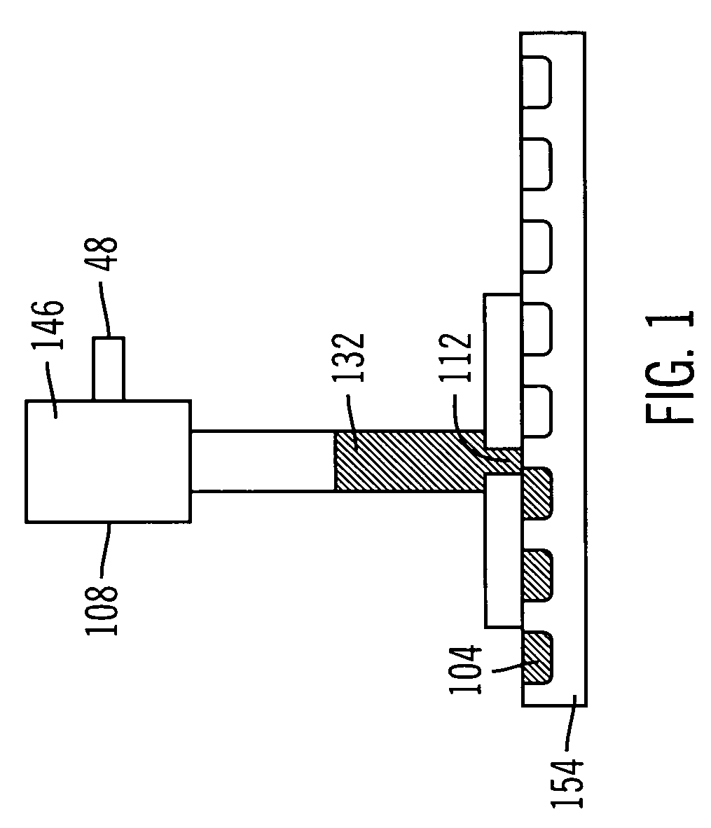
A system, method, and apparatus of providing conductive bonding material into a plurality of cavities in a circuit supporting substrate is disclosed. The method comprises placing a fill head in substantial contact with a circuit supporting substrate. The circuit supporting substrate includes at least one cavity. A linear motion or a rotational motion is provided to at least one of the circuit supporting substrate and the fill head while the fill head is in substantial contact with the circuit supporting substrate. Conductive bonding material is forced out of the fill head toward the circuit supporting substrate. The conductive bonding material is provided into the at least one cavity contemporaneous with the at least one cavity being in proximity to the fill head.

Description

CROSS REFERENCE TO RELATED APPLICATION[0001]The present patent application is related to co-pending and commonly owned U.S. patent application Ser. No. 11 / 409,242, entitled “Universal Mold For Injection Molding Of Solder”, U.S. patent application Ser. No. 11 / 409,232, entitled “Rotational Fill Techniques For Injection Molding Of Solder”, and U.S. patent application Ser. No. 11 / 409,233, entitled “Fill Head For Injection Molding Of Solder”, all filed on even date with the present patent application, their entire teachings of which being hereby incorporated by reference.FIELD OF THE INVENTION [0002]The present invention generally relates to the field of placement of conductive bonding material such as solder on electronic pads, and more particularly relates to placement of the conductive bonding material directly onto a circuit supporting substrate.BACKGROUND OF THE INVENTION[0003]In modern semiconductor devices, the ever increasing device density and decreasing device dimensions demand...

Claims


Application Information

Patent Timeline
Patent Type & Authority Patents(United States)
IPC IPC(8): B23K31/02
CPCB23K3/0607H05K3/3484H05K3/4038B23K2201/42H05K2203/0568H05K2201/09472H05K2203/0126H05K2203/043H05K2201/0305B23K2101/42H05K3/3485
Inventor CORDES, STEVEN A.GRUBER, PETER A.KNICKERBOCKER, JOHN U.SPEIDELL, JAMES L.
Owner TAIWAN SEMICON MFG CO LTD
Learn More