Plasma processing apparatus
a processing apparatus and plasma technology, applied in the field of plasma processing apparatus, can solve the problems of variation in process amount and insufficient synthesis of plasma, and achieve the effects of improving the electric field of the electromagnetic field entering directly from the slot antenna, improving the strength of the electric field as the synthesis of two components, and improving the electric field generating efficiency of the electromagnetic field
- Summary
- Abstract
- Description
- Claims
- Application Information
AI Technical Summary
Benefits of technology
Problems solved by technology
Method used
Image
Examples
first embodiment
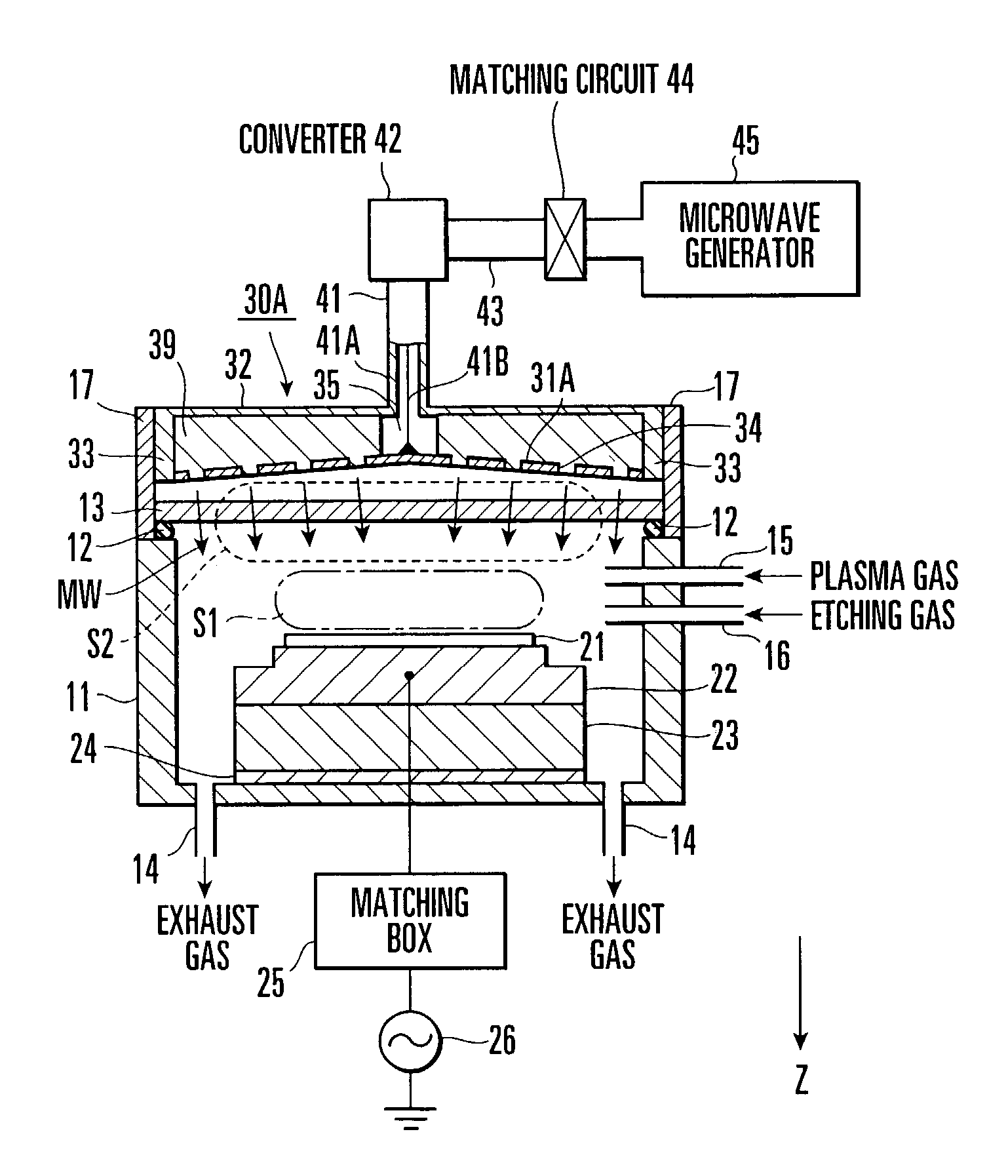
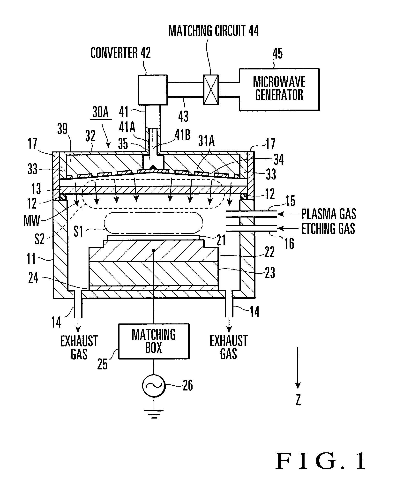
[0046]An embodiment in which the present invention is applied to an etching apparatus will be described. FIG. 1 is a view showing the arrangement of an etching apparatus according to the first embodiment of the present invention. FIG. 1 shows the sectional structure of part of the arrangement. For the sake of descriptive convenience, the vertical direction is defined as the Z-axis direction.
[0047]The etching apparatus shown in FIG. 1 has a cylindrical processing vessel 11 with an upper opening. The processing vessel 11 is made of a conductor such as aluminum. A flat plate-like dielectric plate (first dielectric member) 13 is horizontally arranged in the upper opening of the processing vessel 11. A quartz glass or a ceramic material (e.g., Al2O3 or AlN) with a thickness of about 20 mm to 30 mm is used to form the dielectric plate 13. A seal member 12 such as an O-ring is disposed at the bonding portion between the processing vessel 11 and dielectric plate 13. This assures the hermeti...
second embodiment
[0094]FIG. 11 shows the arrangement of an etching apparatus according to the second embodiment of the present invention. In FIG. 11, the same portions as in FIG. 1 are denoted by the same reference numerals, and a description thereof will be omitted when necessary.
[0095]In a radial antenna 30 used in this etching apparatus, a first conductive plate 31 constituting the radiation surface and a second waveguide 32 which forms a radial waveguide together with the conductive plate 31 are formed of parallel plates. The conductive plates 31 and 32 are arranged horizontally. A dielectric plate (first dielectric member) 13A opposed to the radiation surface of the radial antenna 30 forms a dome. Hence, the dielectric plate 13A has a surface inclining with respect to the radiation surface of the radial antenna 30. The dielectric plate 13A has a shape which is symmetrical with respect to the central axis. A cylindrical spacer 18 is interposed between the dielectric plate 13A and radial antenna ...
third embodiment
[0100]So far cases using radial antennas have been described. The present invention is not limited to them, and the same effect can be obtained by using another slot antenna, e.g., a cavity antenna with slots formed in the antenna lower surface. FIG. 12 shows the arrangement of an etching apparatus according to the third embodiment of the present invention to which a cavity antenna is applied. In FIG. 12, the same portions as in FIG. 1 are denoted by the same reference numerals, and a description thereof will be omitted when necessary. FIG. 13 is a plan view of the radiation surface of the cavity antenna.
[0101]A cavity antenna 70A is formed of a first conductive plate 71A constituting the radiation surface, a second conductive plate 72 arranged above the conductive plate 71A to oppose it, and a ring member 73 for closing the edges of the conductive plates 71A and 72. The conductive plates 71A and 72, and the ring member 73 are made of a conductor such as copper or aluminum.
[0102]The...
PUM
| Property | Measurement | Unit |
|---|---|---|
| wavelength | aaaaa | aaaaa |
| thickness | aaaaa | aaaaa |
| frequency | aaaaa | aaaaa |
Abstract
Description
Claims
Application Information
 - R&D
- Intellectual Property
- Life Sciences
- Materials
- Tech Scout
- Unparalleled Data Quality
- Higher Quality Content
- 60% Fewer Hallucinations
Browse by: Latest US Patents, China's latest patents, Technical Efficacy Thesaurus, Application Domain, Technology Topic, Popular Technical Reports.
© 2025 PatSnap. All rights reserved.Legal|Privacy policy|Modern Slavery Act Transparency Statement|Sitemap|About US| Contact US: help@patsnap.com


