
Method of fabricating a CMOS device with dual metal gate electrodes

a technology of gate oxide layer and cmos device, which is applied in the direction of basic electric elements, semiconductor devices, electrical equipment, etc., can solve the problems of gate oxide layer thickness increase, cmos device scale to smaller dimensions,

Inactive Publication Date: 2008-01-08
AGENCY FOR SCI TECH & RES +1
View PDF7 Cites 30 Cited by
  • Summary
  • Abstract
  • Description
  • Claims
  • Application Information

AI Technical Summary

Problems solved by technology

However, problems arise as the CMOS device is scaled to smaller dimensions.
High resistivity, reduced inversion charge density and transconductance, and undesirable depletion of doped polysilicon gate electrodes can occur, resulting in a detrimental increase in the thickness of the gate oxide layers.
There is also a problem with boron penetration by diffusion from the polysilicon into thin gate oxide layers.
However, current dual metal gate technology has unsolved problems in process integration, especially in the procedure of lithographically masking and removing the first metal of the dual metal gates deposited on a portion of a wafer without generating etching damage to the gate dielectric.
Unfortunately the etching chemical solutions can also attack and remove a portion of the gate dielectric.
This is a practical obstacle in the use of dual metal gate technology in production, even if the right metals are successfully identified.
However, the ion implantation can damage the gate dielectric, resulting in degradation of gate dielectric performance.

Method used


Image

  • Method of fabricating a CMOS device with dual metal gate electrodes
  • Method of fabricating a CMOS device with dual metal gate electrodes
  • Method of fabricating a CMOS device with dual metal gate electrodes

Examples


Embodiment Construction

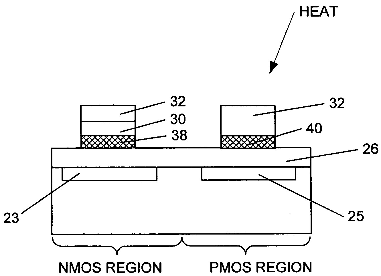
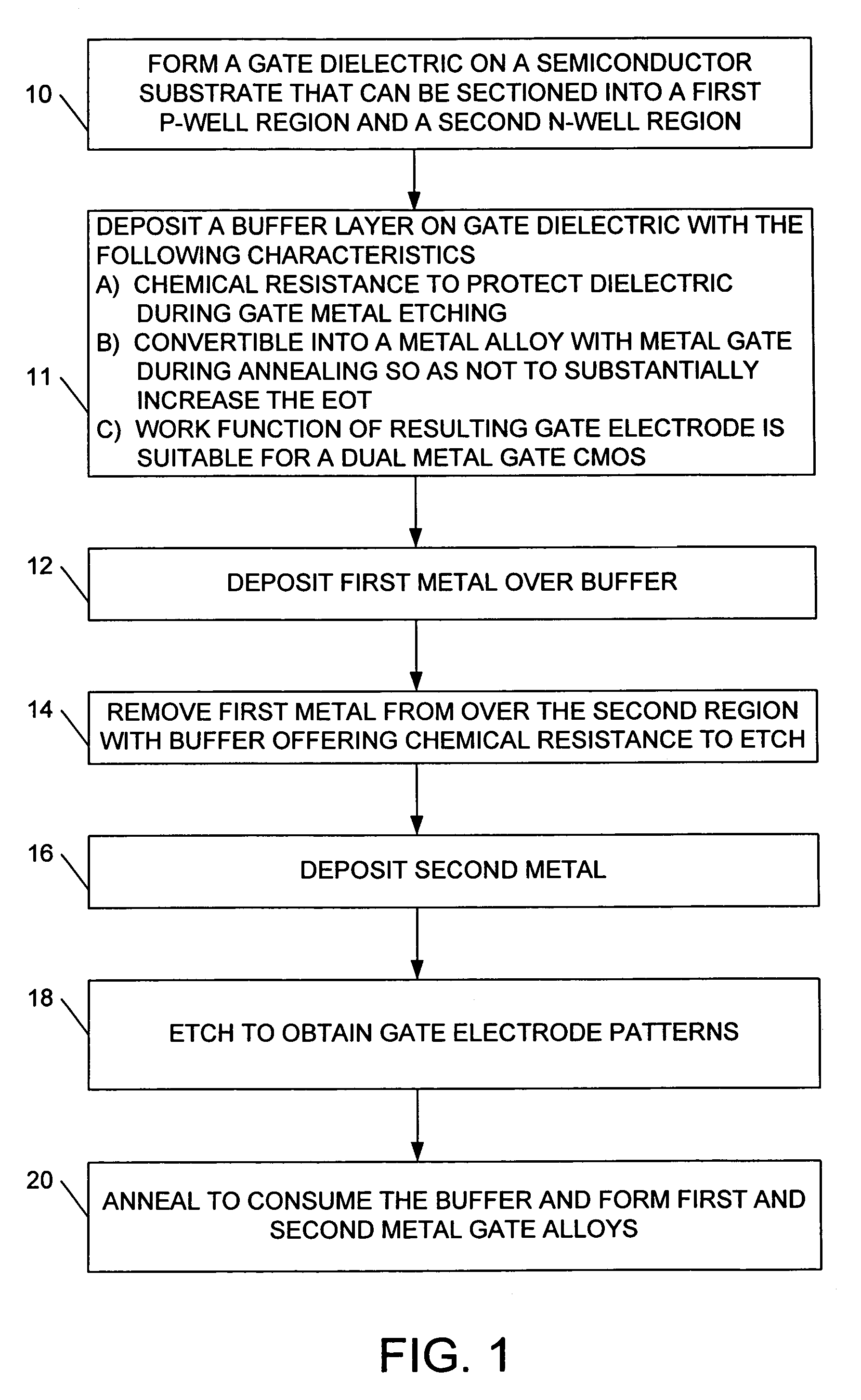
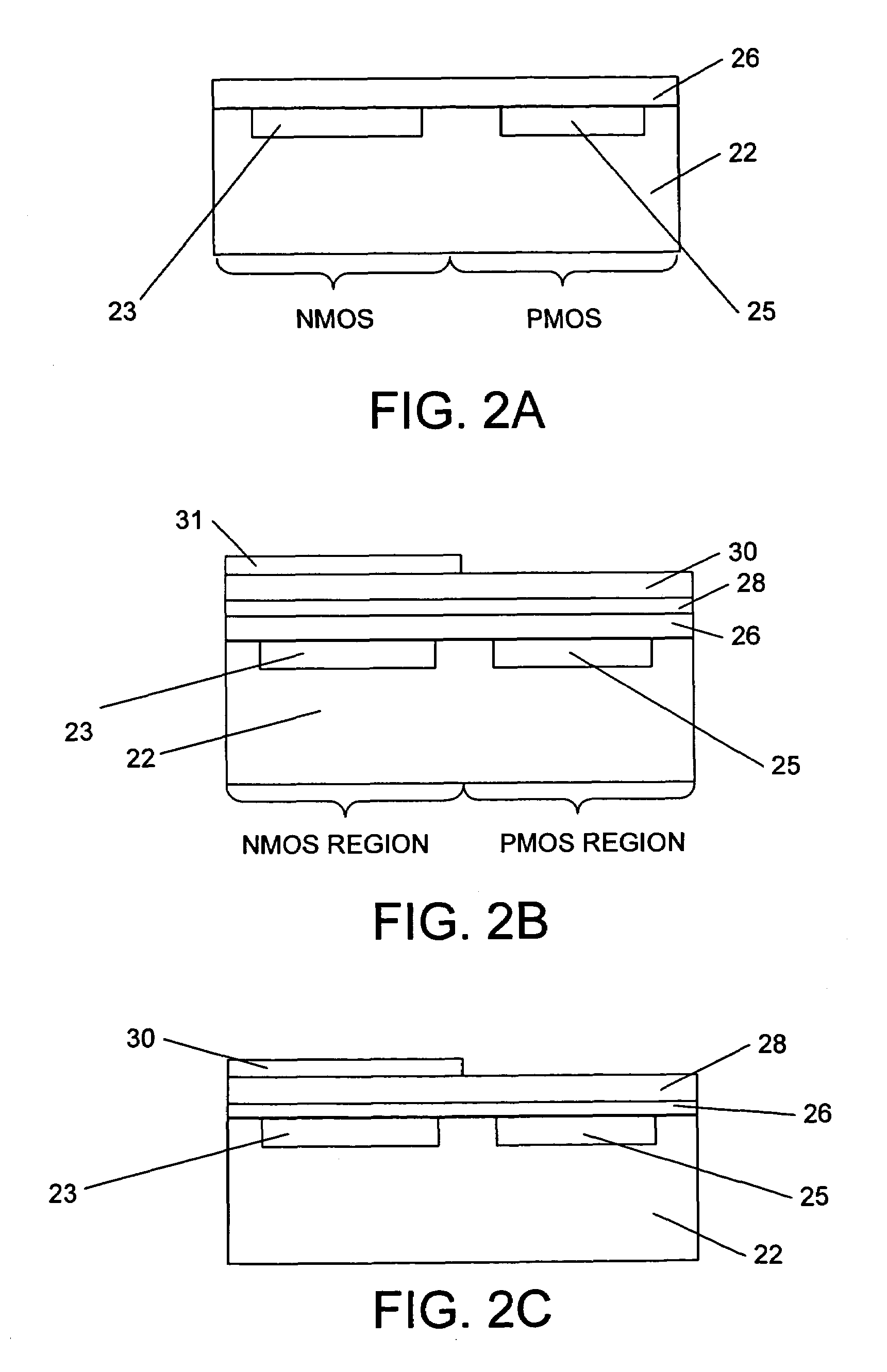
[0019]The method of the present invention is illustrated in the flow chart of FIG. 1. The process / method fabricates dual metal gate electrodes of a CMOS device. This method allows each metal gate electrode to have its optimal work function, namely 4.4 v for NMOS and 4.9 v for PMOS. The process begins (block 10) with forming a gate dielectric 26 on a substrate 22 which has a p-well region and n-well region for use in the formation of NMOSFET and PMOSFET devices in a CMOS. In a preferred embodiment the gate dielectric is thermally grown SiO2. A buffer layer 28 is then deposited (block 11) on the gate dielectric 26 of the CMOS p and n-well structures. Methods for depositing the buffer layer include physical vapor deposition (PVD), chemical vapor deposition (CVD), atomic layer deposition (ALD), and sputtering. The buffer layer material is selected to meet three criteria: (a) It must be chemically resistant to protect the underlying gate dielectric from exposure to an etchant used during...


PUM

PropertyMeasurementUnit
thicknessaaaaaaaaaa
temperatureaaaaaaaaaa
thicknessaaaaaaaaaa

Abstract

A method of constructing a dual metal gate CMOS structure that uses an ultra thin aluminum nitride (AINx) buffer layer between the metal gate and gate dielectric during processing for preventing the gate dielectric from being exposed in the metal etching process. After the unwanted gate metal is etched away, the CMOS structure is annealed. During the annealing, the buffer layer is completely consumed through reaction with the metal gate and a new metal alloy is formed, resulting in only a minimal increase in the equivalent oxide thickness. The buffer layer and gate metals play a key role in determining the work functions of the metal / dielectric interface, since the work functions of the original gate metals are modified as a result of the annealing process.

Description

BACKGROUND OF THE INVENTION[0001]The present application claims priority from U.S. provisional patent application Ser. No. 60 / 464,936 filed Apr. 22, 2003.FIELD OF THE INVENTION[0002]The present invention relates generally to methods of fabricating CMOS devices and more particularly to a method of fabricating a CMOS device with dual metal gate electrodes using a consumable thin buffer layer between the metal gate and the gate dielectric.BRIEF DESCRIPTION OF THE PRIOR ART[0003]In the construction of CMOS devices, doped polysilicon is commonly used for gate electrodes. Polysilicon is convenient because it can be doped to achieved the desired work functions in the two CMOS GATES. However, problems arise as the CMOS device is scaled to smaller dimensions. High resistivity, reduced inversion charge density and transconductance, and undesirable depletion of doped polysilicon gate electrodes can occur, resulting in a detrimental increase in the thickness of the gate oxide layers. There is a...

Claims


Application Information

Patent Timeline
Patent Type & Authority Patents(United States)
IPC IPC(8): H01L21/8238H01L21/28H01L29/49H01L29/51
CPCH01L21/28079H01L21/823842H01L29/495H01L29/513H01L29/517H01L29/518
Inventor PARK, CHANG SEOCHO, BYUNG JINBALASUBRAMANIAN, NARAYANAN T.
Owner AGENCY FOR SCI TECH & RES
Learn More