Method for silicon based dielectric chemical vapor deposition
- Summary
- Abstract
- Description
- Claims
- Application Information
AI Technical Summary
Benefits of technology
Problems solved by technology
Method used
Image
Examples
Embodiment Construction
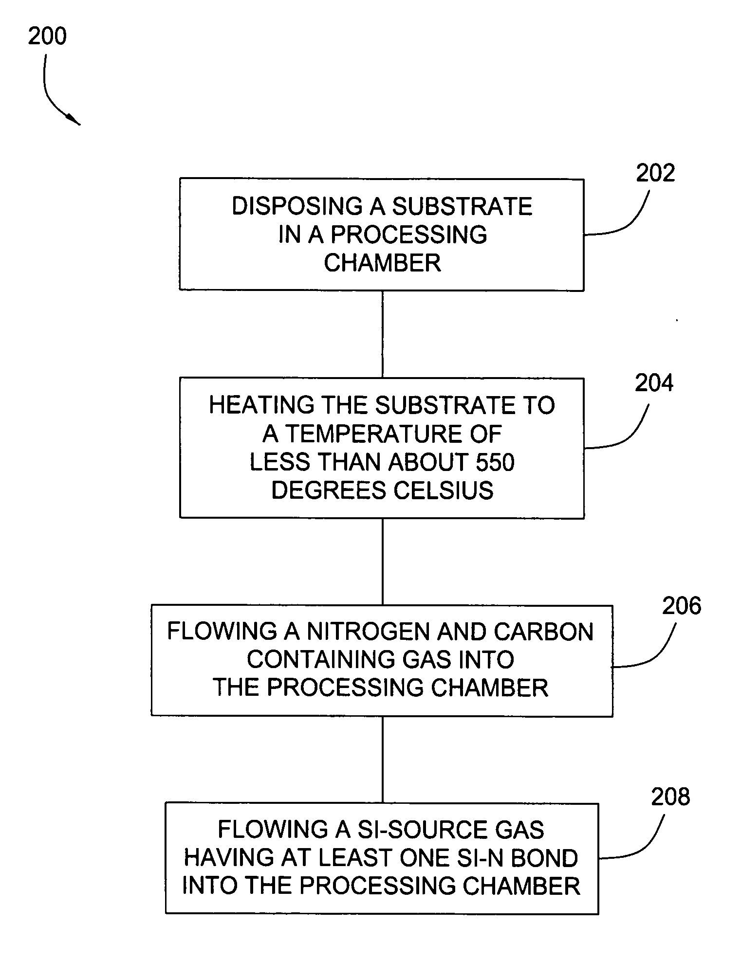
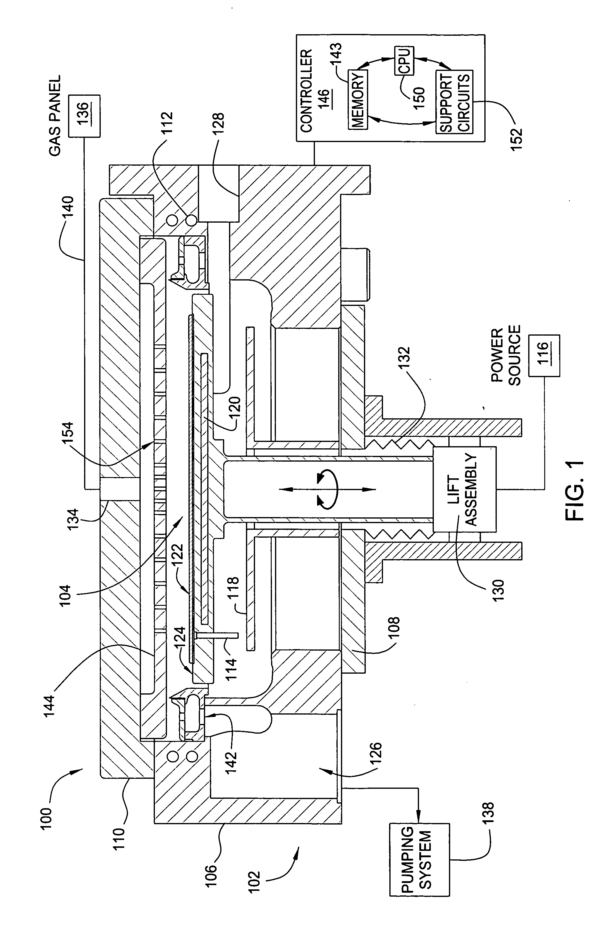
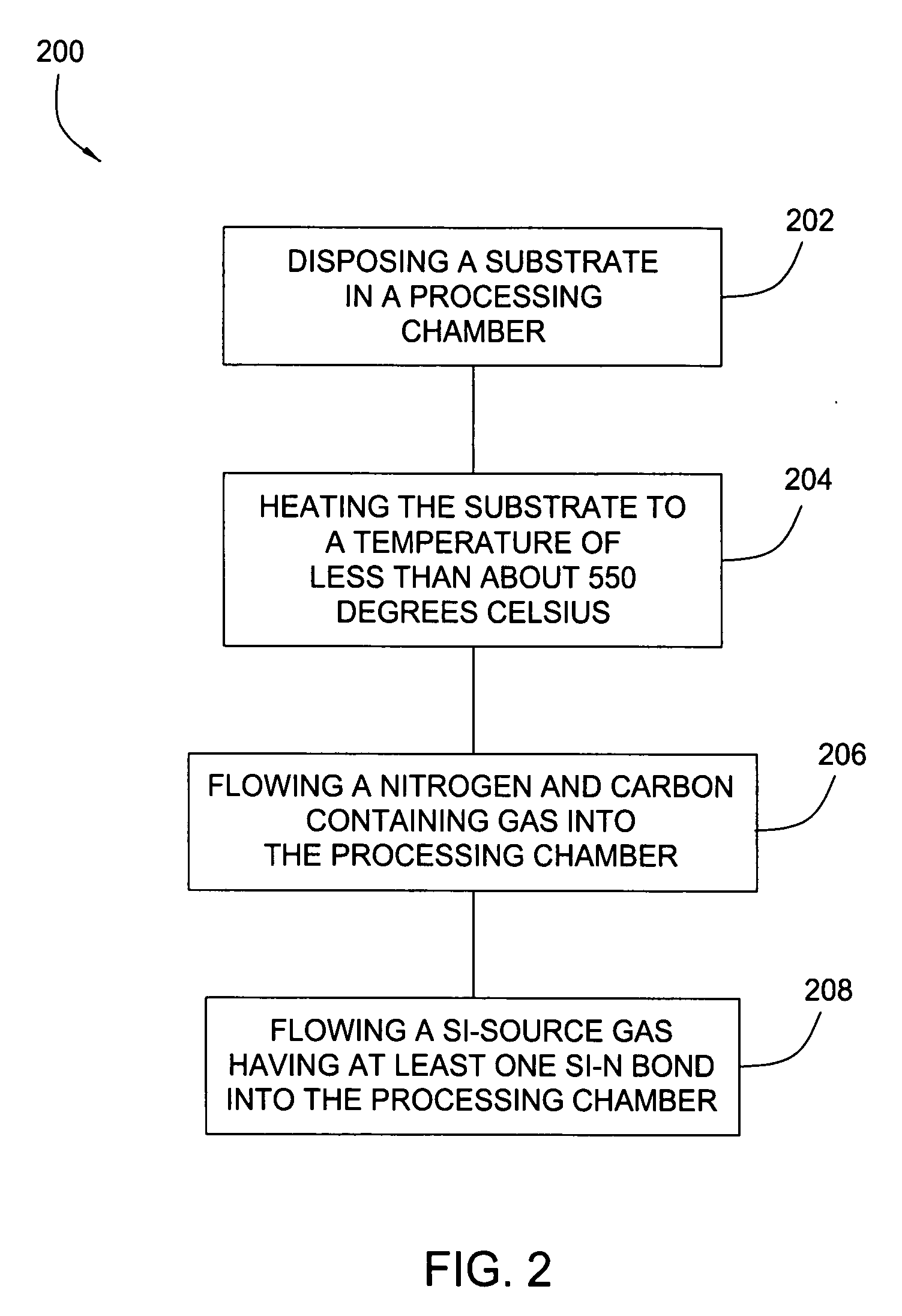
[0013] Embodiments of the invention provide a method for depositing a silicon-containing film, such as silicon nitride and the like, on a substrate utilizing temperatures less than about 550 degrees Celsius. Although the invention is described with reference to a single wafer thermal-chemical vapor deposition (processing) chamber 100 illustrated in FIG. 1, it is contemplated that the method may be beneficially practiced in other deposition systems, including batch deposition systems. One processing chamber in which the silicon nitride deposition process may be performed is a SiNgen®Plus chamber, available from Applied Materials, Inc., of Santa Clara, Calif. Examples of other systems which may be adapted to practice the invention include the TELFORMULA batch furnace available from Tokyo Electron Limited; the FLEXSTAR® mini-batch silicon deposition system available from Applied Materials, Inc.; and the EPSILON® Single-Wafer Epitaxial Reactors from ASM International N.V., among others....
PUM
| Property | Measurement | Unit |
|---|---|---|
| Temperature | aaaaa | aaaaa |
| Temperature | aaaaa | aaaaa |
| Temperature | aaaaa | aaaaa |
Abstract
Description
Claims
Application Information
 - R&D
- Intellectual Property
- Life Sciences
- Materials
- Tech Scout
- Unparalleled Data Quality
- Higher Quality Content
- 60% Fewer Hallucinations
Browse by: Latest US Patents, China's latest patents, Technical Efficacy Thesaurus, Application Domain, Technology Topic, Popular Technical Reports.
© 2025 PatSnap. All rights reserved.Legal|Privacy policy|Modern Slavery Act Transparency Statement|Sitemap|About US| Contact US: help@patsnap.com


