
Method for controlling properties of conformal silica nanolaminates formed by rapid vapor deposition

a technology of conformal silica nanolaminates and vapor deposition, which is applied in the direction of basic electric elements, semiconductor/solid-state device manufacturing, electric apparatus, etc., can solve the problems of reducing budgets, void-free filling of high aspect ratio spaces (ar>3.0:1) becoming increasingly difficult, and reducing dimensions

Active Publication Date: 2007-11-20
NOVELLUS SYSTEMS
View PDF72 Cites 67 Cited by
  • Summary
  • Abstract
  • Description
  • Claims
  • Application Information

AI Technical Summary

Benefits of technology

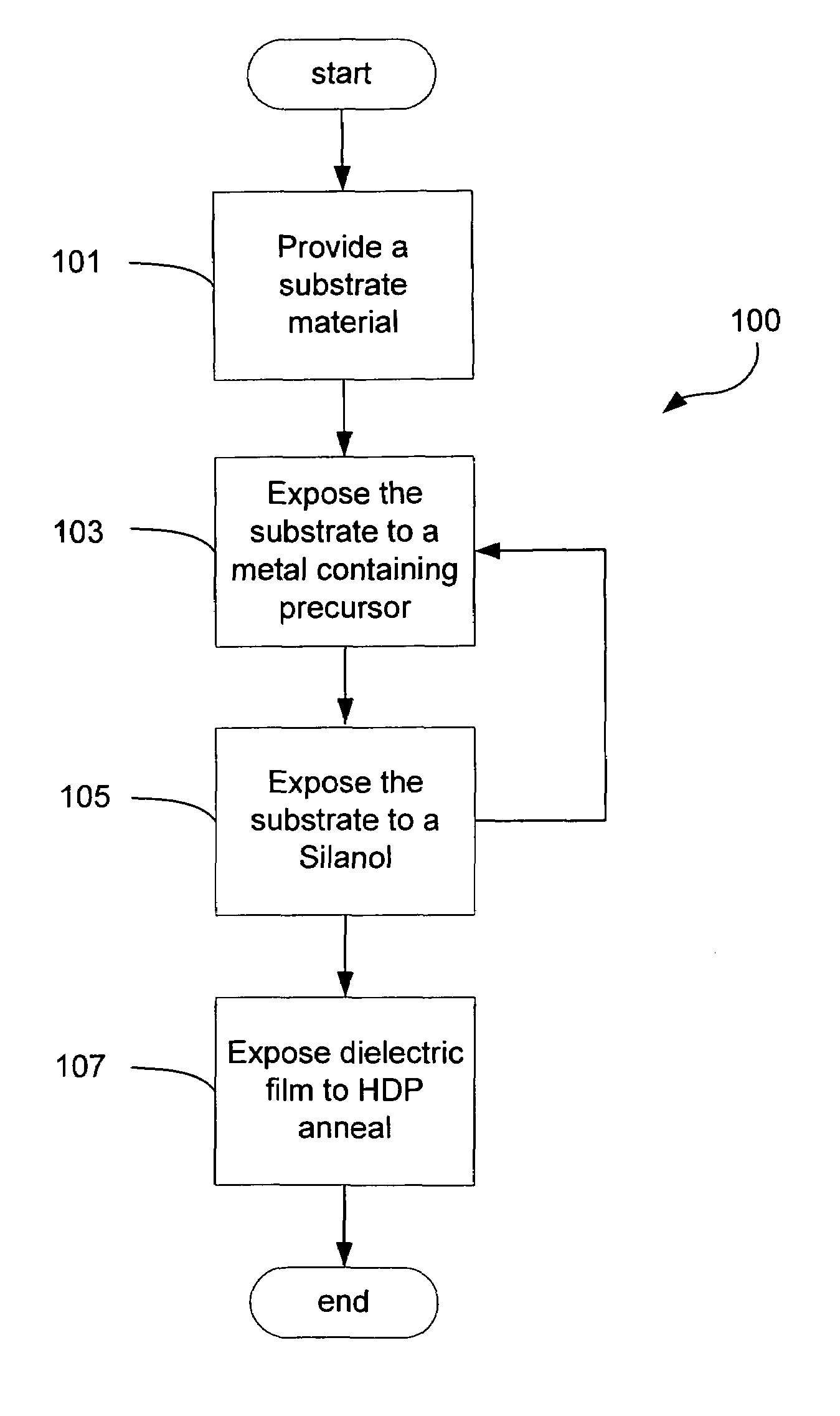
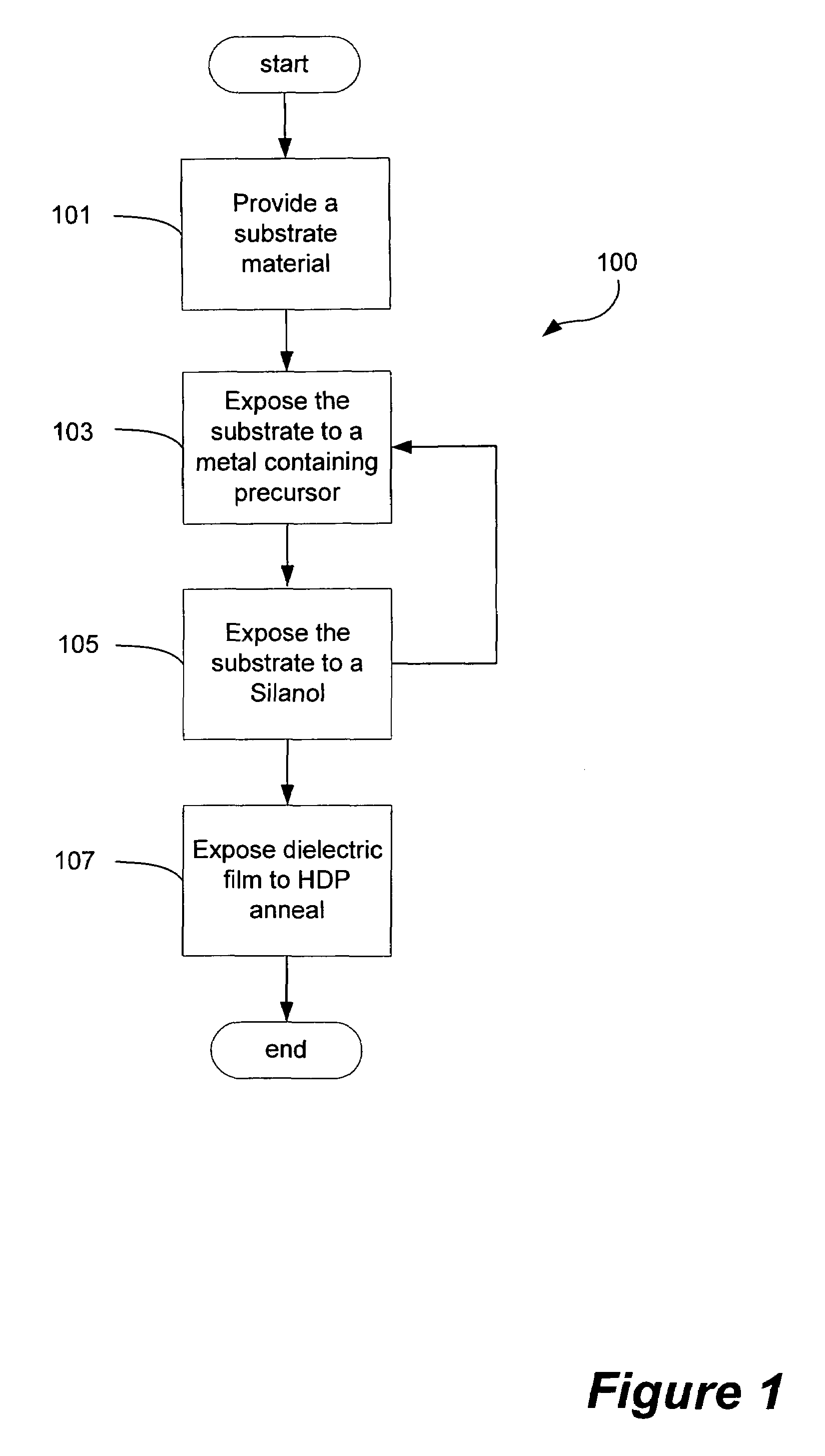
[0006]The present invention provides a method for using a low temperature (i.e., below 500° C.) HDP (high density plasma)-based anneal process to improve the mechanical properties of a dielectric film. This method is applicable to semiconductor gap-fill applications, such as inter-metal dielectric (IMD) layers, premetal dielectric (PMD) and shallow trench isolation (STI).
[0007]The invention provides a method for using RVD techniques to produce a highly conformal dielectric film onto a substrate, followed by an HDP anneal step in an oxidizing environment which improves the properties of the film while maintaining a sufficiently low temperature such that damage to underlying structures is avoided.

Problems solved by technology

As device dimensions shrink and thermal budgets are reduced, void-free filling of high aspect ratio spaces (AR>3.0:1) becomes increasingly difficult due to limitations of existing deposition processes.
For structures representative of the 65 nm and 45 nm technology nodes, engineering the gap-fill process becomes structure dependent, hence the process needs to be reoptimized, a task of considerable complexity, every time a new structure needs to be filled.
One drawback, however, to ALD is that the deposition rates are very low.
These processes are unacceptably slow in some applications in the manufacturing environment.
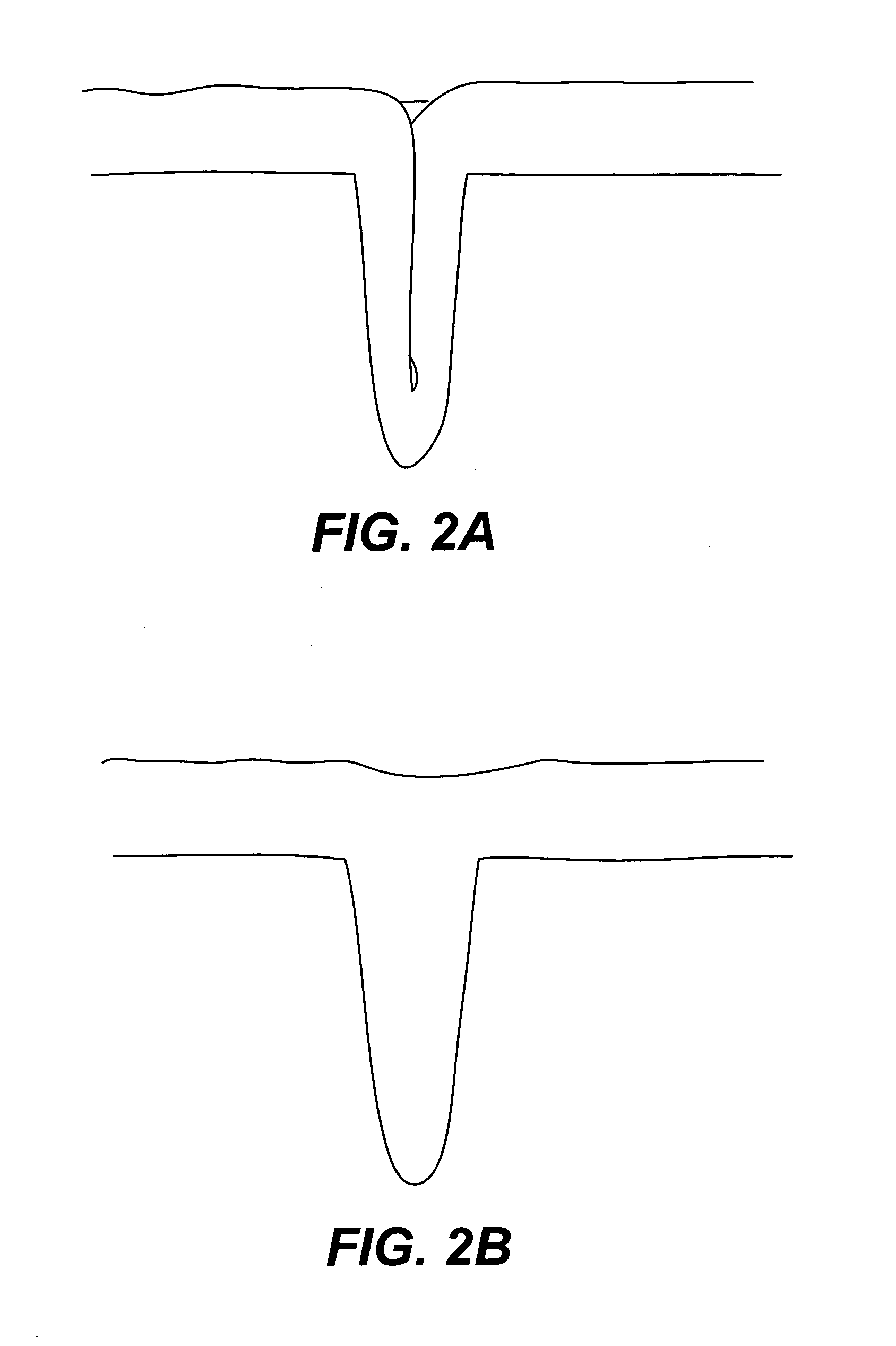
Moreover, the conformal nature of the process results in the formation of seams in filled trenches, which may allow attack by post gap fill wet etch (HF-based) in the seam.
In pre-metal dielectric (PMD) applications, for example, where a layer of silica is applied over gates that have been previously built-up on a substrate, there is an inherent temperature limitation due to the material used to construct the gates (usually a metal silicide such as a nickel silicide.)
At temperatures above about 400-500° C., the gate silicide may become discontinuous, thereby increasing the resistance of the circuit and leading to performance problems.

Method used


Image

  • Method for controlling properties of conformal silica nanolaminates formed by rapid vapor deposition
  • Method for controlling properties of conformal silica nanolaminates formed by rapid vapor deposition
  • Method for controlling properties of conformal silica nanolaminates formed by rapid vapor deposition

Examples


example 1

O2 Gas HDP Anneal

[0058]Time: 700 s[0059]LF Power: 5750 W[0060]Gas flow rate: 250 sccm[0061]Avg. Temperature: 469° C.[0062]Stress, Post Anneal: 0.537 dyn / cm2 [0063]k, Post Anneal: 3.87[0064]WERR, Post Anneal: 1.76[0065]% Film Shrinkage: 3.06

example 2

Argon Gas HDP Anneal

[0066]Time: 700 s[0067]LF Power: 5750 W[0068]Gas flow rate: 250 sccm[0069]Avg. Temperature: 469° C.[0070]Stress, Post Anneal: 2.53 dyn / cm2 [0071]k, Post Anneal: 3.86[0072]WERR, Post Anneal: 2.77[0073]% Film Shrinkage: 12.15

[0074]While not wishing to be limited by theory, it is believed that these differences are due to cross-linking in the densified PDL film. Note also that film stress variation measured before and after the anneal is consistent with the shrinkage measurements, i.e., in the case of the Argon anneal, there is more film shrinkage and more tensile stress after the anneal than in the O2 anneal. However, in both cases, reduced dielectric constant values indicate that H2O has been removed from the film. This is substantiated further by the FTIR spectra shown in FIGS. 5A and B, which show an increase in the size of the Si—O peak post-anneal (at 1058-1062 cm−1) and in the disappearance of the Si—OH peak at 3641 cm−1.

[0075]FIG. 6 is a plot of % film shrin...


PUM

PropertyMeasurementUnit
temperatureaaaaaaaaaa
timeaaaaaaaaaa

Abstract

A method employing atomic layer deposition rapid vapor deposition (RVD) conformally deposits a dielectric material on small features of a substrate surface. The resulting dielectric film is then annealed using a high density plasma (HDP) at a temperature under 500° C. in an oxidizing environment. The method includes the following three principal operations: exposing a substrate surface to an aluminum-containing precursor gas to form a substantially saturated layer of aluminum-containing precursor on the substrate surface; exposing the substrate surface to a silicon-containing precursor gas to form the dielectric film; and annealing the dielectric film in a low temperature oxygen-containing high density plasma. The resulting film has improved mechanical properties, including minimized seams, improved WERR, and low intrinsic stress, comparable to a high temperature annealing process (˜800° C.), but without exceeding the thermal budget limitations of advanced devices.

Description

BACKGROUND OF THE INVENTION[0001]It is often necessary in semiconductor processing to fill a high aspect ratio gap with insulating material. One example of a high aspect ratio trench encountered in semi-conductor processing is in the formation of shallow trench isolation (STI). As device dimensions shrink and thermal budgets are reduced, void-free filling of high aspect ratio spaces (AR>3.0:1) becomes increasingly difficult due to limitations of existing deposition processes. The deposition of doped or undoped silicon dioxide assisted by high density plasma CVD, a directional (bottom-up) CVD process, is the method currently used for high aspect ratio (AR) gap-fill. Evolving semiconductor device designs and dramatically reduced feature sizes have resulted in several applications where HDP processes are challenged in filling the high aspect ratio structures (AR>7:1) using existing technology (see, for example, U.S. Pat. No. 6,030,881). For structures representative of the 65 nm ...

Claims


Application Information

Patent Timeline
Patent Type & Authority Patents(United States)
IPC IPC(8): H01L21/76
CPCH01L21/76224H01L21/3141H01L21/02274H01L21/0228H01L21/02216H01L21/0234
Inventor PAPASOULIOTIS, GEORGE D.TARAFDAR, RAIHAN M.RULKENS, RONHAUSMANN, DENNIS M.TOBIN, JEFFTIPTON, ADRIANNE K.NIE, BUNSEN
Owner NOVELLUS SYSTEMS
Learn More