Compound semiconductor device and manufacturing method thereof

a semiconductor device and manufacturing method technology, applied in semiconductor devices, semiconductor/solid-state device details, electrical devices, etc., can solve the problems of cracking on pad portions, increasing the number of processes and costs,

Active Publication Date: 2007-11-13
SEMICON COMPONENTS IND LLC
View PDF7 Cites 7 Cited by
  • Summary
  • Abstract
  • Description
  • Claims
  • Application Information

AI Technical Summary

Benefits of technology

[0147]In the second place, since the high concentration impurity region is provided below the pad electrode so as to protrude out of the pad electrode, it is possible to suppress a depletion layer which extends from the pad electrode toward the substrate. That is, it is possible to ensure sufficient isolation even in the case of the structure without the nitride film as similar to the conventional technique.
[0148]In the third place, the high concentration impurity region may be separated from the pad electrode and provided on the substrate around the pad electrode. Accordingly, even in the structure configured to contact the pad electrode solely made of the pad metal layer directly to the substrate, it is possible to ensure isolation by small spaces between the respective formation elements.
[0026]The present invention also provides a method of manufacturing a compound semiconductor device. The method includes providing a compound semiconductor substrate, forming a high concentration impurity region and an channel layer in the substrate, forming a gate electrode made of a first metal on the channel layer, forming a pad electrode made of a second metal so that the second metal is in contact with the substrate, the pad electrode being adjacent the high concentration impurity region, and bonding a bonding wire to the pad electrode.
[0150]In the fifth place, it is possible to form the FET having the buried gate electrode without disposing the gate metal layer, which is hardened by being buried below the pad electrode. Therefore, it is possible to provide the method of manufacturing a compound semiconductor device capable of enhancing characteristics of the FET and furthermore suppressing defects at the time of bonding.
[0151]In the sixth place, since the high concentration impurity region is formed on the substrate below the pad electrode, it is possible to provide the method of manufacturing a compound semiconductor device capable of suppressing a depletion layer which extends from the pad electrode and enhancing isolation.
[0152]In the seventh place, the high concentration impurity region may be separated from the pad electrode and provided on the surface of the substrate around the pad electrode. Accordingly, even in the structure configured to contact the pad electrode solely made of the pad metal layer directly to the substrate, it is possible to realize the method of manufacturing a compound semiconductor device capable of ensuring isolation by small spaces between the respective formation elements.
[0154]In the ninth place, the insulating film is formed on the source region and the drain region in the step of forming the source region and the drain region. In this way, it is possible to perform mask alignment of the first source electrode, the first drain electrode, and the gate electrode directly with the source region and the drain region, and thereby to form a FET having small channel resistance.

Problems solved by technology

Such an aspect may cause a lot of problems such as occurrence of damages by electrostatic discharge due to low insulation strength or deterioration in isolation due to leakage of a high frequency signal.
However, the nitride film is hard and therefore causes cracks on pad portions by pressure at the time of bonding.
However, a gold plating process causes increases in the number of processes and in costs.
The gold plating process causes increases in the number of processes and in costs.
For this reason, problems such as degradation in bonding adhesion or gouges on the substrate occur and lead to reduction in yields or deterioration

Method used


Image

  • Compound semiconductor device and manufacturing method thereof
  • Compound semiconductor device and manufacturing method thereof
  • Compound semiconductor device and manufacturing method thereof

Examples


first embodiment

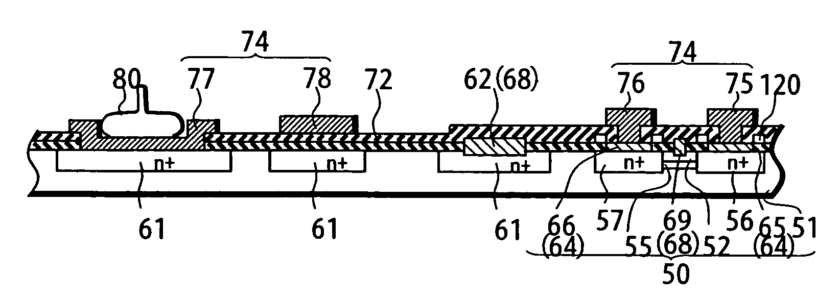
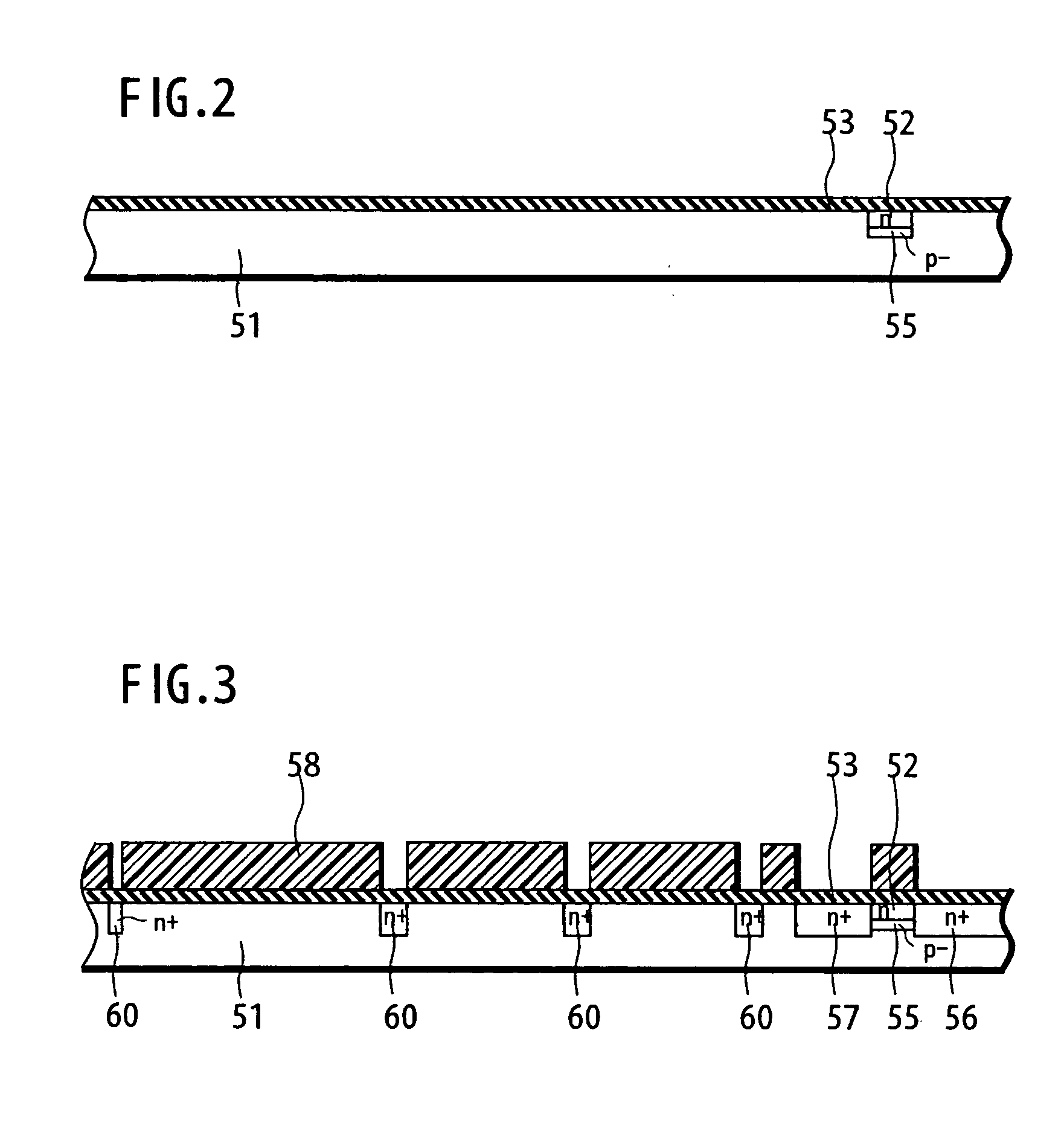
[0104]First to third steps (FIG. 8A): Same as the first embodiment, after forming channel layer 52 on a substrate 51, resist 58 is formed and a photolithography process is performed to selectively form openings in the resist layer 58 in the respective formation regions for the source region 56, the drain region 57, high concentration impurity region 60, and alignment mark 130. Subsequently, ions of an n-type impurity (29Si+, impurity concentration equal to or above 1×1017 cm−3) are implanted on the surface of the substrate 51 in the formation regions for the source region 56, the drain region 57, the high concentration impurity region 60, and the alignment mark 130 while using this resist layer 58 as a mask.

[0105]In this way, the n+-type source region 56 and drain region 57 are formed adjacently to a channel layer 52. Meanwhile, the high concentration impurity region 60 is formed on the surface of the substrate 51 around the formation region for the gate wiring 62. At the same time,...

second embodiment

[0116]In the second embodiment, the high concentration impurity region 60 having the floating potential is also formed below the pad wiring 78. In this case, the nitride film 72, the oxide film 120, and the nitride film 53 are disposed below the pad wiring 78. Accordingly, when the high frequency signal passes through the pad wiring 78, the nitride films 72 and 53 and the oxide film become capacitive elements and the high frequency signal leaks out to the substrate 51. However, by providing the high concentration impurity region 60 having the floating potential to which no direct current potential is applied, it is possible to prevent leakage of the high frequency signal from the pad wiring 78 to the substrate 51 more effectively.

[0117]Here, the high concentration impurity region 60 below the pad electrode 77 may be provided only in the vicinity of the pad electrode 77 and formed into a pattern such that the pad electrode 77 partially contacts the high concentration impurity region ...


PUM

PropertyMeasurementUnit
distanceaaaaaaaaaa
distanceaaaaaaaaaa
concentrationaaaaaaaaaa

Abstract

A pad electrode of a field effect transistor is formed solely of a pad metal layer without providing a gate metal layer. A high concentration impurity region is provided below the pad electrode, and the pad electrode is directly contacted to a substrate. Predetermined isolation is ensured by the high concentration impurity region. Accordingly, in a structure not requiring a nitride film as similar to the related art, it is possible to avoid defects upon wire boding attributing to hardening of the gate metal layer. Therefore, in the case of a buried gate electrode structure for enhancing characteristics of the field effect transistor, it is possible to enhance reliability and yields.

Description

BACKGROUND OF THE INVENTION[0001]1. Field of the Invention[0002]The present invention relates to a compound semiconductor device and a manufacturing method of the same, particularly, to a compound semiconductor device and a manufacturing method of the same which are capable of enhancing characteristics of field effect transistors and reducing defects in wire bonding.[0003]2. Background Art[0004]Mobile communication devices such as mobile telephones often use microwaves in a gigahertz range and frequently use switching devices to switch antennas or transmitting / receiving for switching those high frequency signals (see Japanese Patent Application Publication No. Hei 9-181642, for example). Such devices often use field effect transistors (hereinafter referred to as FETs) using gallium arsenide (GaAs) to deal with microwave signals. In this concern, development of monolithic microwave integrated circuits (MMICs) configured to integrate the above-mentioned switching circuits are now in p...

Claims


Application Information

Patent Timeline
Patent Type & Authority Patents(United States)
IPC IPC(8): H01L23/48H01L27/095H01L21/28H01L21/3205H01L21/338H01L21/60H01L21/768H01L21/822H01L23/485H01L23/52H01L23/522H01L27/04H01L27/06H01L29/417H01L29/423H01L29/812H01L31/0328
CPCH01L24/03H01L24/05H01L24/06H01L24/48H01L27/0605H01L29/423H01L2924/1306H01L2224/48669H01L2224/48666H01L2224/48644H01L2924/00014H01L2924/30105H01L2924/19043H01L2924/1423H01L2924/14H01L2924/10329H01L2924/05042H01L2924/01082H01L2924/01079H01L2924/01078H01L2924/01075H01L24/45H01L2224/04042H01L2224/05599H01L2224/05644H01L2224/05666H01L2224/05669H01L2224/45144H01L2224/48463H01L2924/01004H01L2924/01005H01L2924/01006H01L2924/01012H01L2924/01014H01L2924/01015H01L2924/01022H01L2924/01028H01L2924/01031H01L2924/01033H01L2924/01042H01L2924/01032H01L2924/00H01L2924/12032H01L2924/181H01L29/80
Inventor ASANO, TETSURO
Owner SEMICON COMPONENTS IND LLC
Why Eureka
Try Eureka