Semiconductor device, designing method for semiconductor device, computer-readable medium, and manufacturing method for semiconductor device

a semiconductor device and design method technology, applied in the direction of computer aided design, basic electric elements, instruments, etc., can solve the problem of difficult to keep an area of the wiring layer

Inactive Publication Date: 2010-11-18
RENESAS ELECTRONICS CORP
View PDF2 Cites 3 Cited by
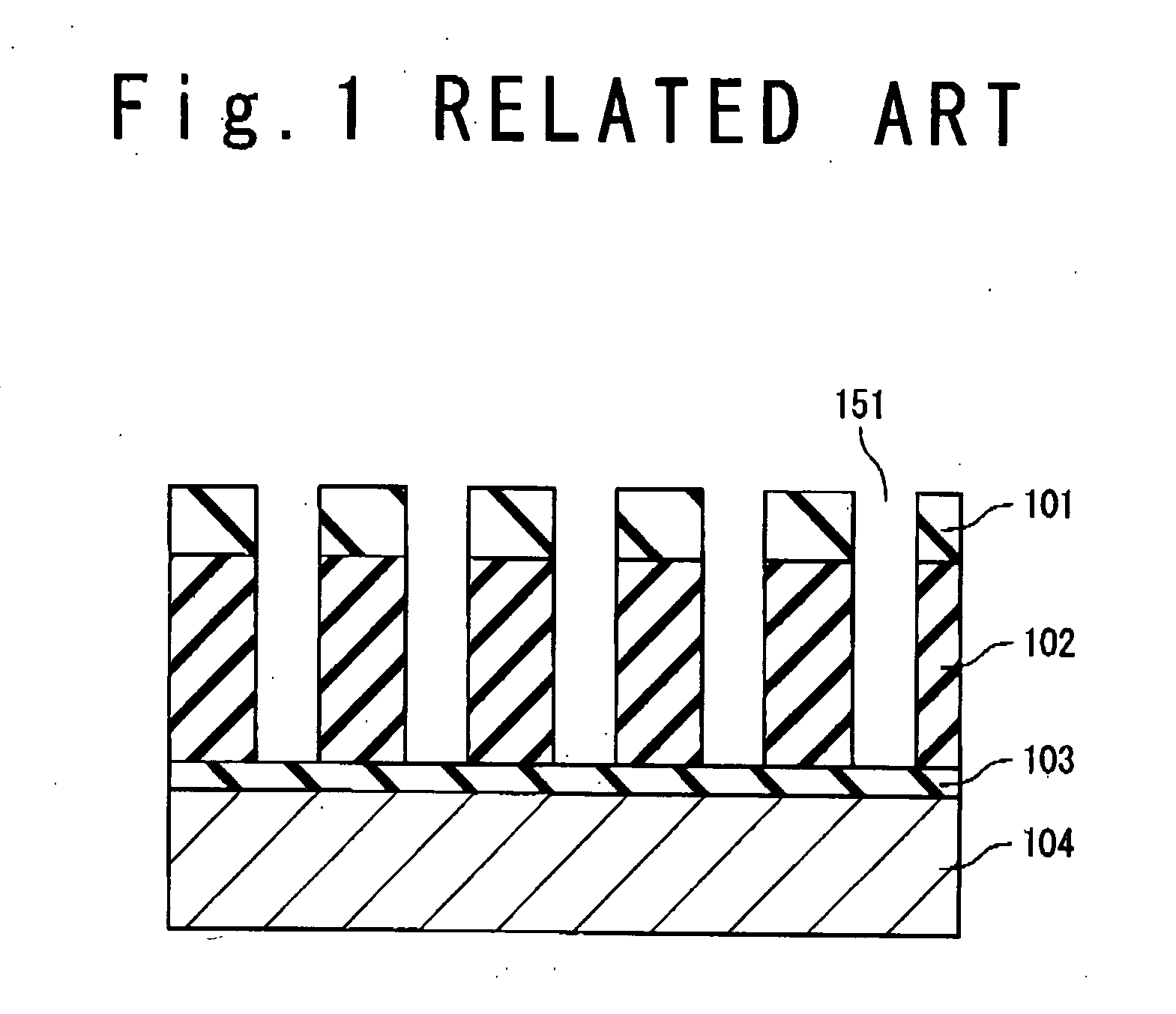
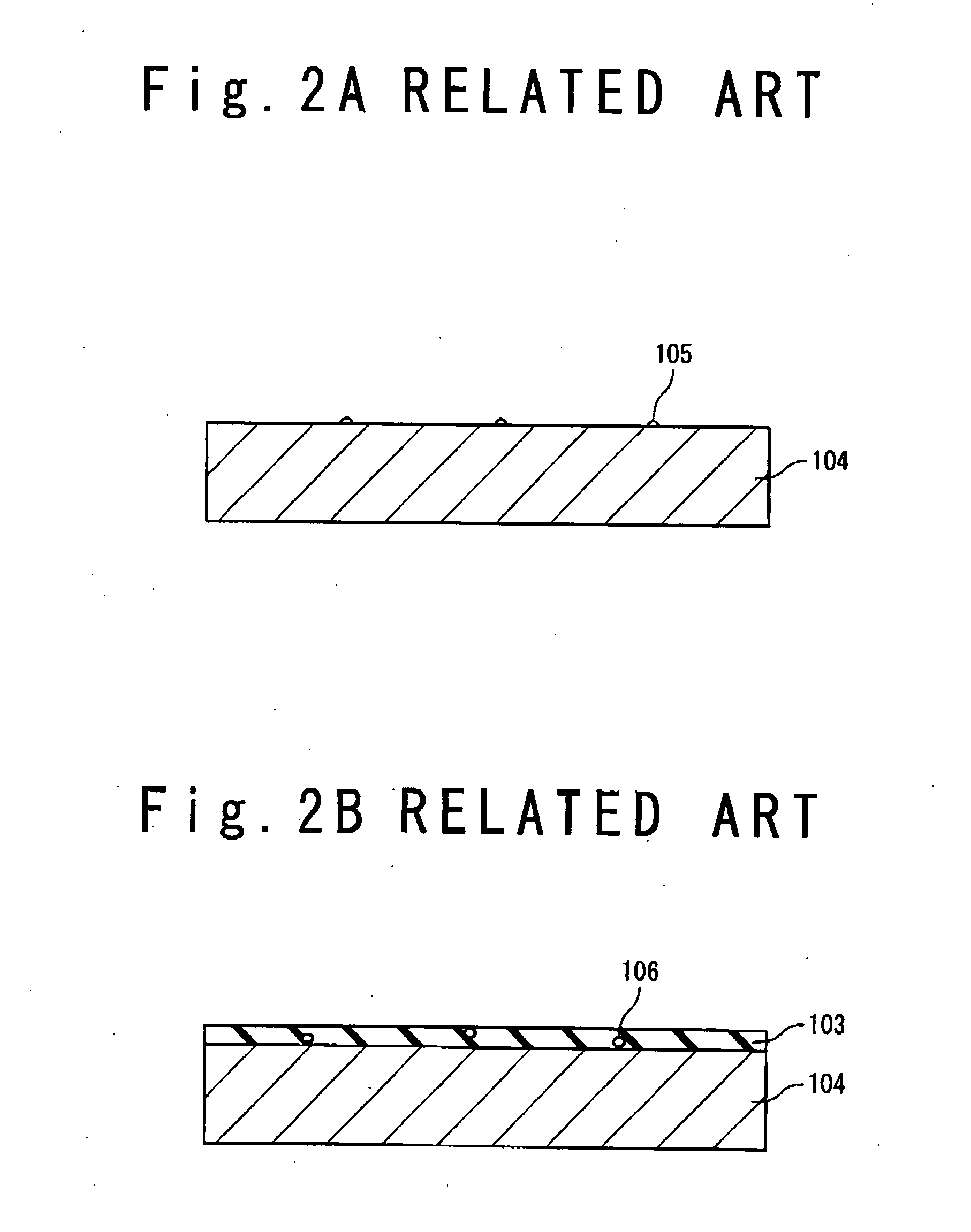
  • Summary
  • Abstract
  • Description
  • Claims
  • Application Information

AI Technical Summary

Benefits of technology

[0025]There can be provided a semiconductor device and a design method for the semiconductor device that suppress a wiring layer from being eluted and oxidized.

Problems solved by technology

In particular, if there is a through-hole that is locally opened, it is difficult to keep an area of the wiring layer, which is an underlying layer to be connected to the through-hole, at a certain value or less with respect to the number of through-holes where an underlying wiring is exposed.

Method used


Image

  • Semiconductor device, designing method for semiconductor device, computer-readable medium, and manufacturing method for semiconductor device
  • Semiconductor device, designing method for semiconductor device, computer-readable medium, and manufacturing method for semiconductor device
  • Semiconductor device, designing method for semiconductor device, computer-readable medium, and manufacturing method for semiconductor device

Examples


first embodiment

[0060]An embodiment of the present invention is described below on the basis of drawings. Note that, in the drawings for describing following embodiments, the same members (and / or portions) are denoted by the same symbols in principle, and their repeat explanation is omitted.

[0061]FIG. 5 is a block diagram exemplifying a configuration of a semiconductor design support device 1 in the first embodiment. The semiconductor design support device 1 includes an information processor 2, input device 3, and output device 4. The information processor 2 is a main body part of the device, which is represented by a computer or the like, and performs information processing at high speed. The information processor 2 is provided with a five basic functions, i.e., input, storage, calculation, control, and output. The information processor 2 performs information processing according to a procedure described in a program. The input device 3 is a man-machine interface represented by a keyboard or mouse...

second embodiment

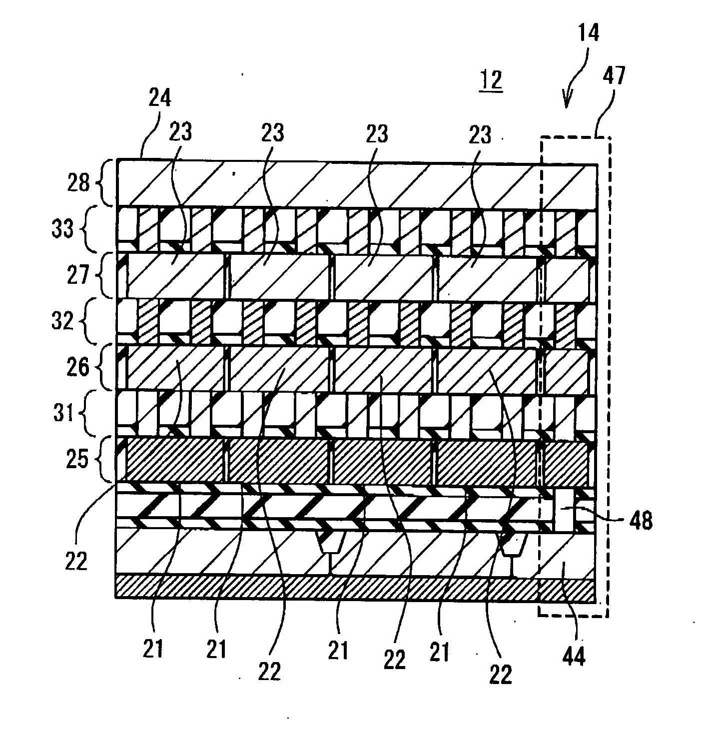
[0084]A second embodiment of the present invention is specifically described below referring to the accompanying drawings. FIG. 10 is a flowchart exemplifying an operation of a semiconductor design support device in the second embodiment. The operation in the second embodiment is different from that in the first embodiment, in which wiring layout is optimized with including not only a wiring of a wiring layer of interest but also a wiring provided in a wiring layer underlying the wiring layer of interest.

[0085]In Step S101, similarly to the first embodiment, through-holes for forming contact holes of multilayer wiring to be designed are specified. Also, wirings having surfaces exposed by the through-holes at the time of manufacturing are specified.

[0086]Then, in Step S201, areas of the specified wiring in a wiring layer and a wiring in an underlying wiring layer are calculated. Here, the underlying wiring layer is underlies the wiring layer including the specified wiring. At this ti...


PUM


Abstract

A designing method for a semiconductor device includes: determining a placement of metal wirings to be connected to contact holes and a placement of through-holes for preparing the contact holes. The determining step includes: specifying areas in one of the metal wirings to be exposed by the through-holes, specifying a capacitance of the metal wirings, and determining the placement of the metal wirings such that damage to the areas is suppressed in a case where electric charges accumulated in the capacitance are transferred from one of the metal wirings to a polar solvent through the areas.

Description

INCORPORATION BY REFERENCE[0001]This application is based upon and claims the benefit of priority from Japanese patent application No. 2009-115819 filed on May 12, 2009, the disclosure of which is incorporated herein in its entirety by reference.BACKGROUND OF THE INVENTION[0002]1. Field of the Invention[0003]The present invention relates to a semiconductor device, a designing method for the semiconductor device, and a semiconductor design supporting program that supports designing the semiconductor device.[0004]2. Description of Related Art[0005]As a technique related to manufacturing of a semiconductor device including a multilayer wiring layer, a damascene method is known. In the damascene method, an opening portion (through-hole) is formed through an interlayer film provided on a circuit board by a method such as dry etching or plasma asking. After the opening portion (through-hole) is formed, residue formed during the etching process is removed by cleaning by using a chemical so...

Claims


Application Information

Patent Timeline
Patent Type & Authority Applications(United States)
IPC IPC(8): H01L23/522G06F17/50H01L21/768
CPCG06F17/5077H01L21/76802H01L21/76814H01L23/5222H01L2924/0002H01L23/528H01L2924/00G06F30/394
Inventor HAMANAKA, NOBUAKI
Owner RENESAS ELECTRONICS CORP
Why Eureka
Try Eureka