
Ferroelectric/paraelectric multilayer thin film, method of forming the same, and high frequency variable device using the same

a multi-layer, high frequency variable technology, applied in the direction of electrical equipment, semiconductor devices, capacitors, etc., can solve the problems of difficult epitaxial growth of a bst thin film, high insertion loss, frequency/phase variable rate, etc., to improve the high frequency response characteristic, small dielectric loss, and high tuning rate of a dielectric constan

Inactive Publication Date: 2007-09-25
ELECTRONICS & TELECOMM RES INST
View PDF9 Cites 5 Cited by
  • Summary
  • Abstract
  • Description
  • Claims
  • Application Information

AI Technical Summary

Benefits of technology

The present invention provides a new structure of a ferroelectric / paraelectric multilayer thin film with high tuning rate of dielectric constant and small dielectric loss. The invention also provides a method of forming the thin film for optimizing dielectric properties with lower price. The invention further provides a high frequency variable device with excellent microwaves characteristics, including high speed, low power consumption, and low prices. The ferroelectric / paraelectric multilayer thin film has high tuning rate and small dielectric loss with externally applied voltages, and improves high frequency response characteristic of the high frequency variable device. The invention can be used in high-speed and capacitance next-generation wireless multimedia systems and sensing systems.

Problems solved by technology

However, the most significant problems in the development of the high frequency frequency / phase variable device using such a ferroelectric thin film are their high insertion losses, frequency / phase variable rate, high operation voltage and the like.
However, there is limitation in achieving a BST thin film having properties comparable to dielectric properties of BST single crystal.
Particularly, epitaxial growth of a BST thin film is not easy at a low temperature due to large difference of lattice constants between the BST thin film and oxide single crystal substrate, and further, high strain / stress inside the thin film is known as a main reason to deteriorate a tuning rate of a dielectric constant and dielectric loss.
Because of that, propagation loss of high frequency signals is increased, and a ferroelectric high frequency variable device having effective and excellent characteristics was difficult to realize.

Method used


Image

  • Ferroelectric/paraelectric multilayer thin film, method of forming the same, and high frequency variable device using the same
  • Ferroelectric/paraelectric multilayer thin film, method of forming the same, and high frequency variable device using the same
  • Ferroelectric/paraelectric multilayer thin film, method of forming the same, and high frequency variable device using the same

Examples


Embodiment Construction

[0030]The present invention will now be described more fully hereinafter with reference to the accompanying drawings, in which preferred embodiments of the invention are shown. This invention may, however, be embodied in many different forms and should not be construed as being limited to the embodiments set forth herein. Rather, these embodiments are provided so that this disclosure will be thorough and complete, and will fully convey the scope of the invention to those skilled in the art. Like numbers refer to like elements throughout the specification.

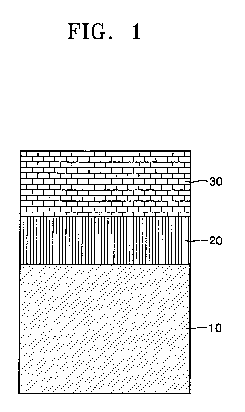
[0031]FIG. 1 is a sectional view illustrating a ferroelectric / paraelectric multilayer thin film according to an embodiment of the present invention.

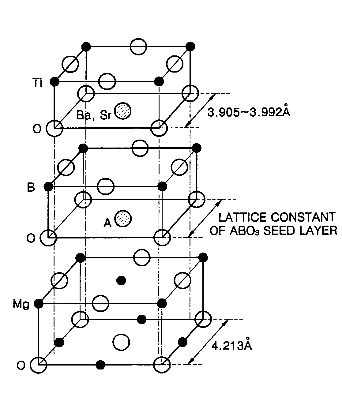
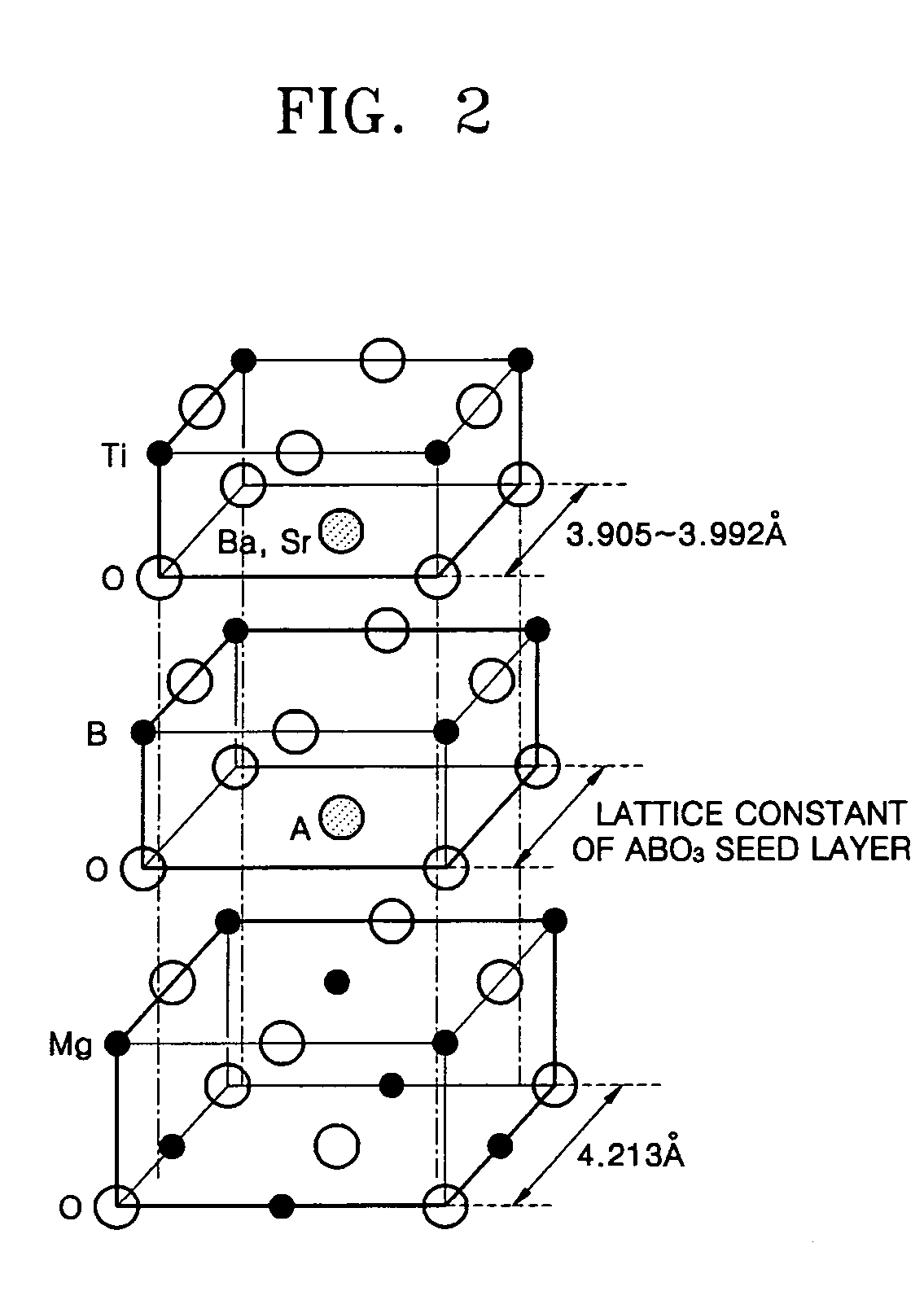
[0032]Referring to FIG. 1, a ferroelectric thin film of the present invention includes a paraelectric seed layer 20, which is composed of perovskite compound represented by a general formula of ABO3 (hereinafter, referred to as “perovskite ABO3 structure”), formed with a predetermined th...


PUM

PropertyMeasurementUnit
thicknessaaaaaaaaaa
thicknessaaaaaaaaaa
dielectric constantaaaaaaaaaa

Abstract

A ferroelectric / paraelectric multilayer thin film having a high tuning rate of a dielectric constant and small dielectric loss to overcome limitations of a tuning rate of a dielectric constant and dielectric loss of a ferroelectric thin film, a method of forming the same, and a high frequency variable device having the ferroelectric / paraelectric multilayer thin film are provided. The ferroelectric / paraelectric multilayer thin film includes a perovskite ABO3 structure paraelectric seed layer formed on a substrate, and an epitaxial ferroelectric (BaxSr1-x)TiO3 thin film formed on the paraelectric seed layer. The high frequency variable device can realize a RF frequency / phase variable device having a high speed, low power consumption, and low prices and excellent microwaves characteristics.

Description

CROSS-REFERENCE TO RELATED PATENT APPLICATION[0001]This application claims the benefit of Korean Patent Application No. 10-2004-0101087, filed on Dec. 3, 2004, in the Korean Intellectual Property Office, the disclosure of which is incorporated herein in its entirety by reference.BACKGROUND OF THE INVENTION[0002]1. Field of the Invention[0003]The present invention relates to a ferroelectric / paraelectric multilayer thin film, a method of forming the same, and a high frequency variable device using the same, and more particularly, to a ferroelectric / paraelectric multilayer thin film composed of a barium-strontium-titanium thin film, a method of forming the same, and a high frequency variable device using the same.[0004]2. Description of the Related Art[0005]Recently, new services, such as high capacity next-generation wideband broadcast, communication, internet-combined mobile wireless multimedia system, ubiquitous communication, sensor system and the like, are realized into actualitie...

Claims


Application Information

Patent Timeline
Patent Type & Authority Patents(United States)
IPC IPC(8): H01L29/76H01L29/94H01L31/00
CPCH01G7/06H01L21/31691H01L28/56H01P1/181H01L21/0226H01L21/022H01L21/02197H01L21/20
Inventor LEE, SU JAEMOON, SEUNG EONRYU, HAN CHEOLKWAK, MIN HWANKANG, KWANG YONG
Owner ELECTRONICS & TELECOMM RES INST
Learn More