Method for writing data into a memory cell of a conductive bridging random access memory, memory circuit and CBRAM memory circuit

a random access memory and memory cell technology, applied in the field of cbram memory circuits, can solve problems such as programming failure, and achieve the effect of reducing voltag

Inactive Publication Date: 2007-08-14
POLARIS INNOVATIONS LTD
View PDF12 Cites 19 Cited by
  • Summary
  • Abstract
  • Description
  • Claims
  • Application Information

AI Technical Summary

Benefits of technology

[0007]The present invention refers to a method for writing data into a memory cell of a conductive bridging random access memory and to a memory circuit comprising memory cells with programmable metallization cells, particularly a CBRAM memory circuit. One embodiment of the present invention provides a method of writing a datum in a memory cell of a conductive bridge random access memory (CBRAM), comprising a plate line, at least three bit lines that are disposed side by side, and at least three memory cells with a programmable metallization cell (PMC) in each of the at least three memory cells, and each of the at least three memory cells is connected to a respective bit line of the at least three bit lines and the plate line. The method comprises applying to a selected bit line, that is connected to a selected memory cell, a writing voltage for the selected memory cell to write a datum in the selected memory cell to change the resistance value of a selected PMC of the selected memory cell, applying to a first neighboring bit line of the selected bit line, wherein the first neighboring bit line is connected to a first neighboring memory cell of the selected memory cell, a writing voltage of the first neighboring memory cell corresponding to a datum stored in the first neighboring memory cell so that data are written in the selected and the first neighboring memory cells during the writing operation of the selected memory cell to reduce voltage crosstalk between the selected bit line and the first neighboring bit line, and applying to a second neighboring bit line of the selected bit line, wherein the second neighboring bit line is connected to a second neighboring memory cell of the selected memory line, a writing voltage of the second neighboring memory cell corresponding to a datum stored in the second neighboring memory cell, so that data are written in the selected, the first neighboring, and the second neighboring memory cells during the writing operation of the selected memory cell to reduce voltage crosstalk between the selected bit line, the first neighboring bit line, and the second neighboring bit line.
[0010]Yet another embodiment of the present invention provides a memory circuit that comprises at least two bit lines that are disposed side by side, at least two memory cells disposed side by side with each of the at least two memory cells connected to a respective bit line of the at least two bit lines, and means of writing a datum to a selected memory cell of the at least two memory cells, wherein during writing the datum to the selected memory cell, the neighboring memory cells of the selected memory cell are written during the same writing operation with data that were stored in the neighboring memory cells prior to the writing operation to reduce voltage crosstalk between the bit lines during the writing operation.

Problems solved by technology

However, voltage crosstalk might occur between the high voltage level of a selected bit line, used for programming a selected PMC cell, and a non-selected (or floating) neighboring bit line that could cause a programming failure.

Method used


Image

  • Method for writing data into a memory cell of a conductive bridging random access memory, memory circuit and CBRAM memory circuit
  • Method for writing data into a memory cell of a conductive bridging random access memory, memory circuit and CBRAM memory circuit
  • Method for writing data into a memory cell of a conductive bridging random access memory, memory circuit and CBRAM memory circuit

Examples


Embodiment Construction

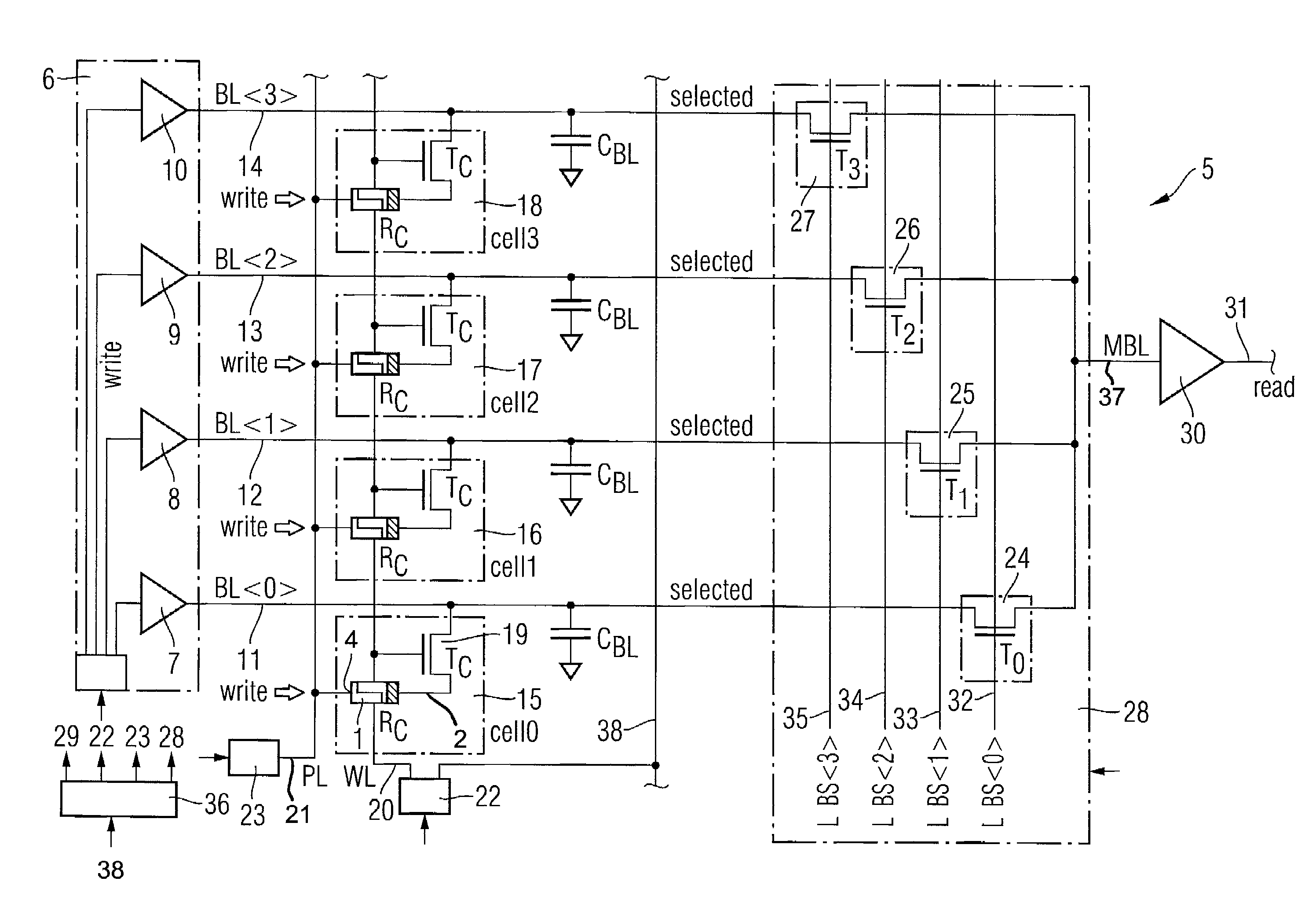
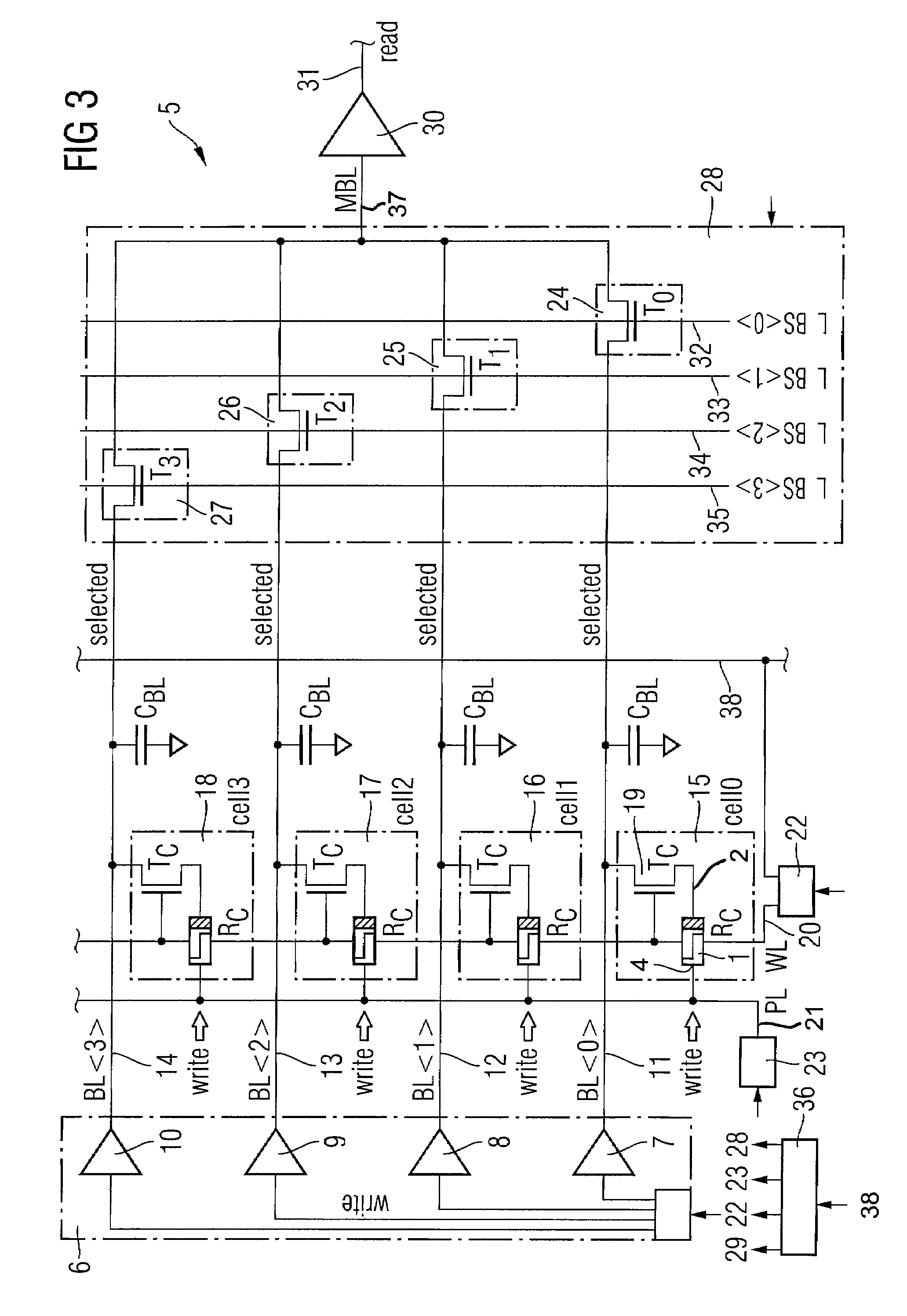
[0016]Embodiments of the present invention provide a method and a memory circuit for holding adjacently arranged bit lines at the writing voltages corresponding to the data stored or corresponding to the data that should be written in the memory cells therein during a writing operation to reduce voltage crosstalk. The concept of the invention can be used in any memory circuit, particularly in a CBRAM memory circuit.

[0017]The present invention may be described in terms of various functional components. It should be appreciated that such functional components may be realized by any number of hardware or structural components configured to perform the specified functions. For example, the present invention may employ various integrated components comprised of various electrical devices, e.g. resistors, transistors, capacitors, diodes and such like, the values of which may be suitably configured for various intended purposes. In addition, the present invention may be practiced in any in...


PUM


Abstract

The present invention refers to a method for writing data into a memory cell of a conductive bridging random access memory and to a memory circuit comprising memory cells with programmable metallization cells, particularly a CBRAM memory circuit. The embodiments of the prevent invention provide a method and a memory circuit for holding adjacently arranged bit lines at writing voltages during a writing operation of a selected memory cell to reduce voltage crosstalk.

Description

BACKGROUND OF THE INVENTION[0001]1. Field of the Invention[0002]The present invention refers to a method for writing data into a memory cell of a conductive bridging random access memory and to a memory circuit comprising memory cells with programmable metallization cells, particularly a CBRAM memory circuit.[0003]2. Description of the Related Art[0004]Memory cells comprising a solid electrolyte material are well known as PMC (programmable metallization cell) memory cells. Memory devices including such PMC memory cells are known as CBRAM (conductive-bridging random access memory) devices. The storing of different states in a PMC memory cell is based on the developing or diminishing of a conductive path in the electrolyte material between electrodes based on an applied electrical field. Although the electrolyte material has a high resistance, the conductive path between electrodes has a low resistance. Thereby, the PMC memory cell can be set to different states depending on the resis...

Claims


Application Information

Patent Timeline
Patent Type & Authority Patents(United States)
IPC IPC(8): G11C11/00
CPCG11C13/0011G11C13/0069G11C2013/009G11C2213/79
Inventor ROEHR, THOMAS
Owner POLARIS INNOVATIONS LTD
Why Eureka
Try Eureka