Substrate processing apparatus and substrate processing method

a substrate processing and substrate technology, applied in the direction of photosensitive material processing, liquid cleaning, coating, etc., can solve the problems of corroding parts, contaminating the semiconductor wafer, and expensive disposal of waste liquid produced by the resist film removal method using the spm solution, so as to reduce the processing time necessary for processing substrates and improve throughput , the effect of high durability

Inactive Publication Date: 2007-06-12
TOKYO ELECTRON LTD +1
View PDF19 Cites 9 Cited by
  • Summary
  • Abstract
  • Description
  • Claims
  • Application Information

AI Technical Summary

Benefits of technology

[0011]The substrate processing apparatus and the substrate processing method of the present invention protect the inner surfaces of the walls of the processing vessel and the component members placed in the processing vessel from corrosive actions of the processing gas. Thus, the substrate processing apparatus has high durability. Since the productio...

Problems solved by technology

The known resist film removing method has problems that particles contained in the chemical liquid adhere to the semiconductor wafer when the semiconductor wafer is immersed in the chemical liquid, and particles removed from the semiconductor wafer and suspended in the chemical liquid adhere to other semiconductor wafers.
The disposal of waste liquid produced by th...

Method used


Image

  • Substrate processing apparatus and substrate processing method
  • Substrate processing apparatus and substrate processing method
  • Substrate processing apparatus and substrate processing method

Examples


Embodiment Construction

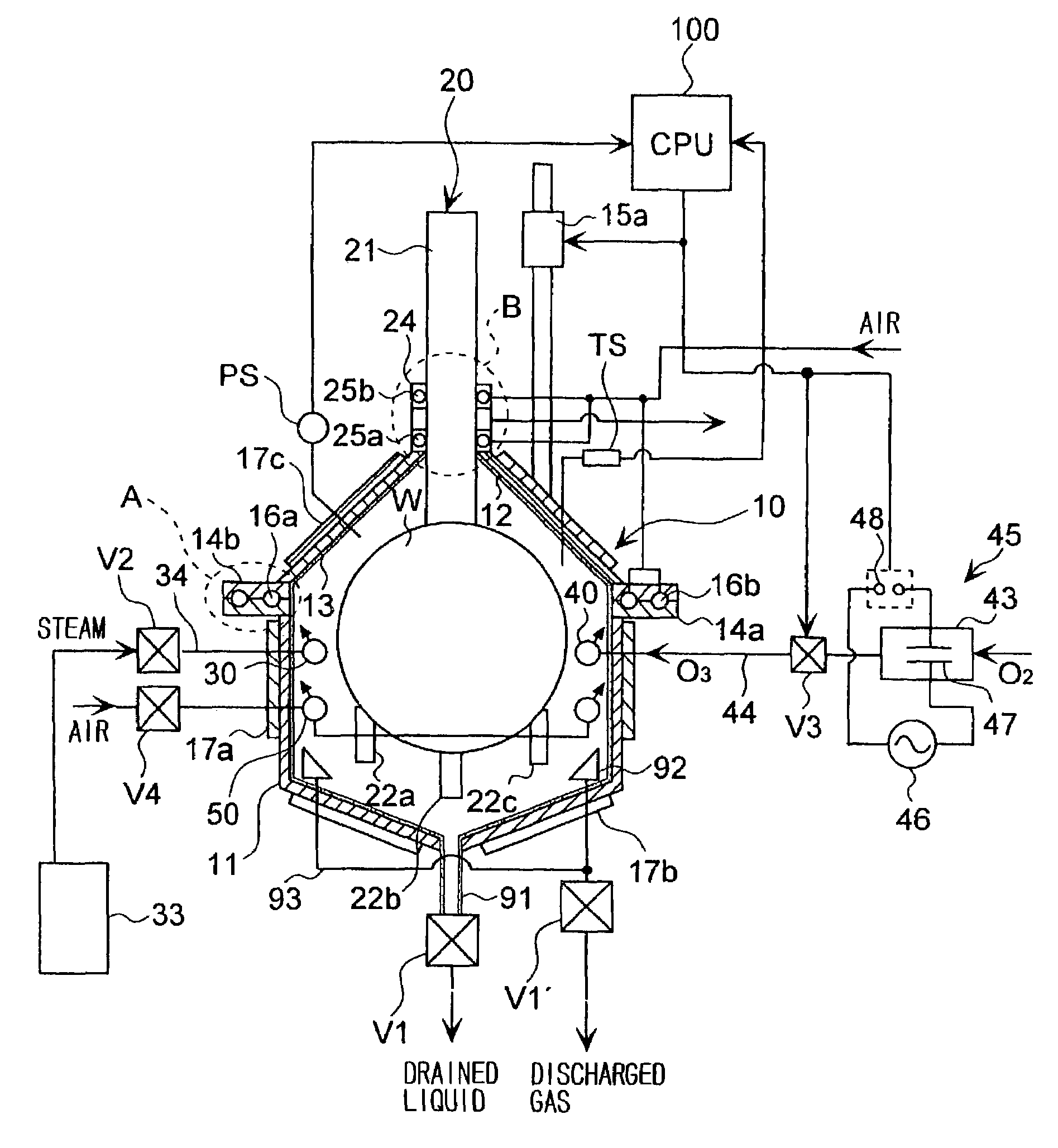
[0022]A resist film removing apparatus 1 in a preferred embodiment according to the present invention will be described as applied to removing useless resist films formed on semiconductor wafers (hereinafter, referred to simply as “wafers”) W by supplying a gas and a vapor to alter the resist film by a mixed gaseous fluid of the gas and the vapor. In this embodiment, the vapor is steam (water vapor, typically pure-water vapor), and the gas is an ozone-containing gas (which is oxygen gas containing ozone gas of a predetermined concentration).

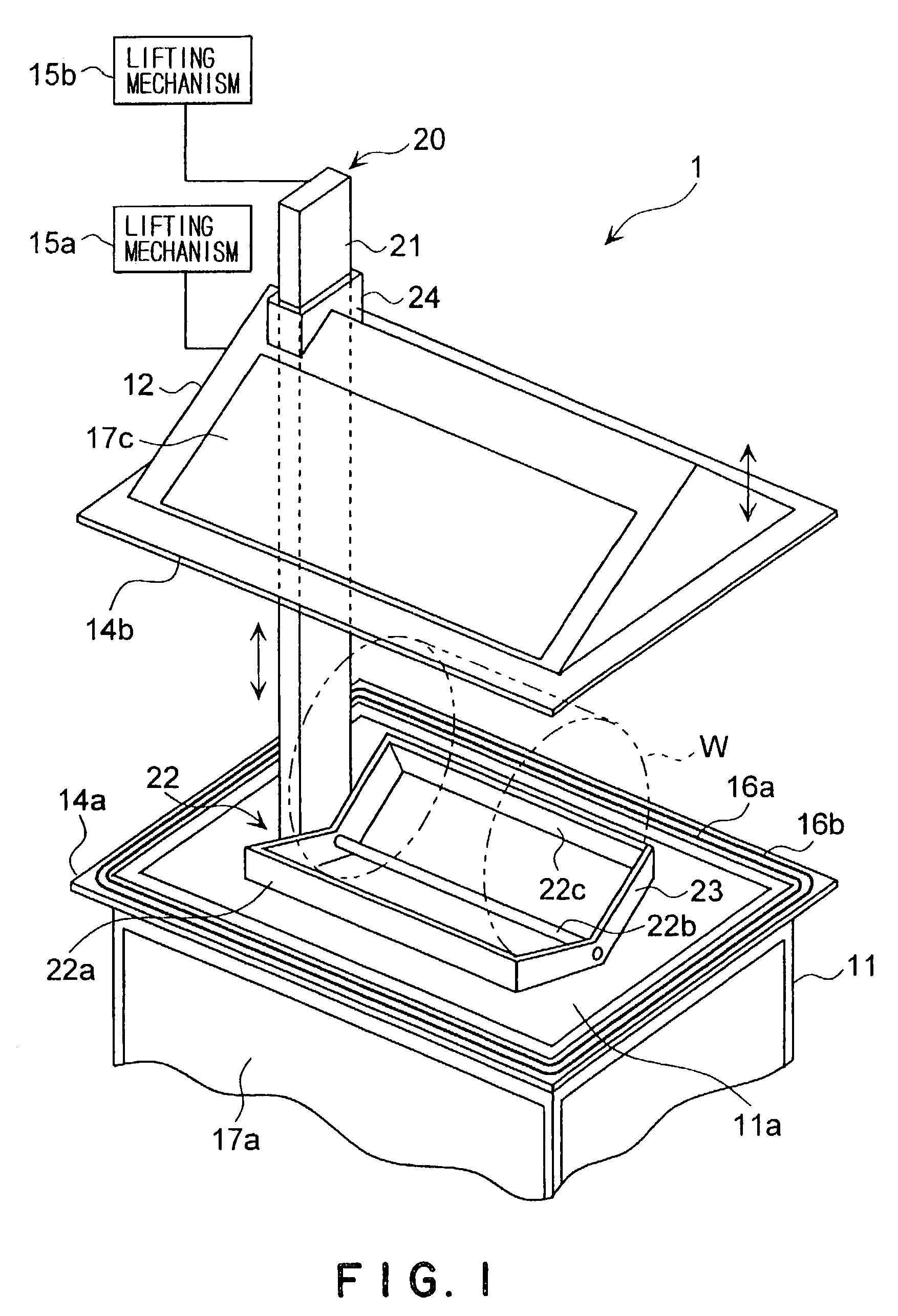
[0023]Referring to FIGS. 1 and 2, the resist film removing apparatus 1 includes: a processing vessel 10 in which wafers W are processed; a wafer guide 20, i.e., a wafer holding device that holds wafers W in the processing vessel 10; a steam jetting nozzle 30 that supplies steam into the processing vessel 10; an ozone-containing gas jetting nozzle 40 that supplies an ozone-containing gas containing ozone (O3) into the processing vessel 10; and air...


PUM

PropertyMeasurementUnit
Temperatureaaaaaaaaaa
Pressureaaaaaaaaaa

Abstract

A substrate processing apparatus removes resist films formed on wafers by holding the wafers in a processing vessel and exposing the wafers to a mixed gaseous fluid of steam and an ozone-containing gas into the processing vessel. The inner surfaces, to be exposed to the mixed gaseous fluid, of the processing vessel and the surfaces, to be exposed to the mixed gaseous fluid, of component members placed in the processing vessel are coated with SiO2 film to protect the same from the corrosive action of the mixed gaseous fluid.

Description

BACKGROUND OF THE INVENTION[0001]1. Field of the Invention[0002]The present invention relates to a substrate processing apparatus and a substrate processing method for processing substrates, such as semiconductor wafers or glass substrates for LCDs (liquid crystal displays), in an atmosphere containing a vapor and a gas.[0003]2. Description of the Related Art[0004]Generally, a semiconductor device fabricating method includes a step of forming a predetermined circuit pattern on-a semiconductor wafer by photolithography. More specifically, a semiconductor device fabricating method includes series of steps of applying a liquid photoresist to a semiconductor wafer cleaned by a cleaning process to form a photoresist film, exposing the photoresist film to a desired light pattern, subjecting the exposed photoresist film to a developing process to form a photoresist mask, subjecting the semiconductor wafer to an etching process and a doping process, and removing the photoresist mask, i.e., ...

Claims


Application Information

Patent Timeline
IPC IPC(8): C23F1/00B08B3/00H01L21/306G03F7/42H01L21/00H01L21/027H01L21/304H01L21/3065H01L21/311H01L21/673
CPCH01L21/31138H01L21/67757H01L21/6708Y10S156/914H01L21/027
Inventor TOSHIMA, TAKAYUKIABE, HITOSHI
Owner TOKYO ELECTRON LTD
Why Eureka
Try Eureka