Composition for forming porous film, porous film and method for forming the same, interlevel insulator film, and semiconductor device
a technology of porous film and insulator, which is applied in the direction of transportation and packaging, coatings, and silicon oxides, can solve the problem that the mechanical strength of the conventional crosslinking agent cannot be achieved, and achieve the effect of reducing the parasitic capacitance of the area around the multilayer interconnection, high-speed operation, and reducing the hygroscopic property of the porous film
- Summary
- Abstract
- Description
- Claims
- Application Information
AI Technical Summary
Benefits of technology
Problems solved by technology
Method used
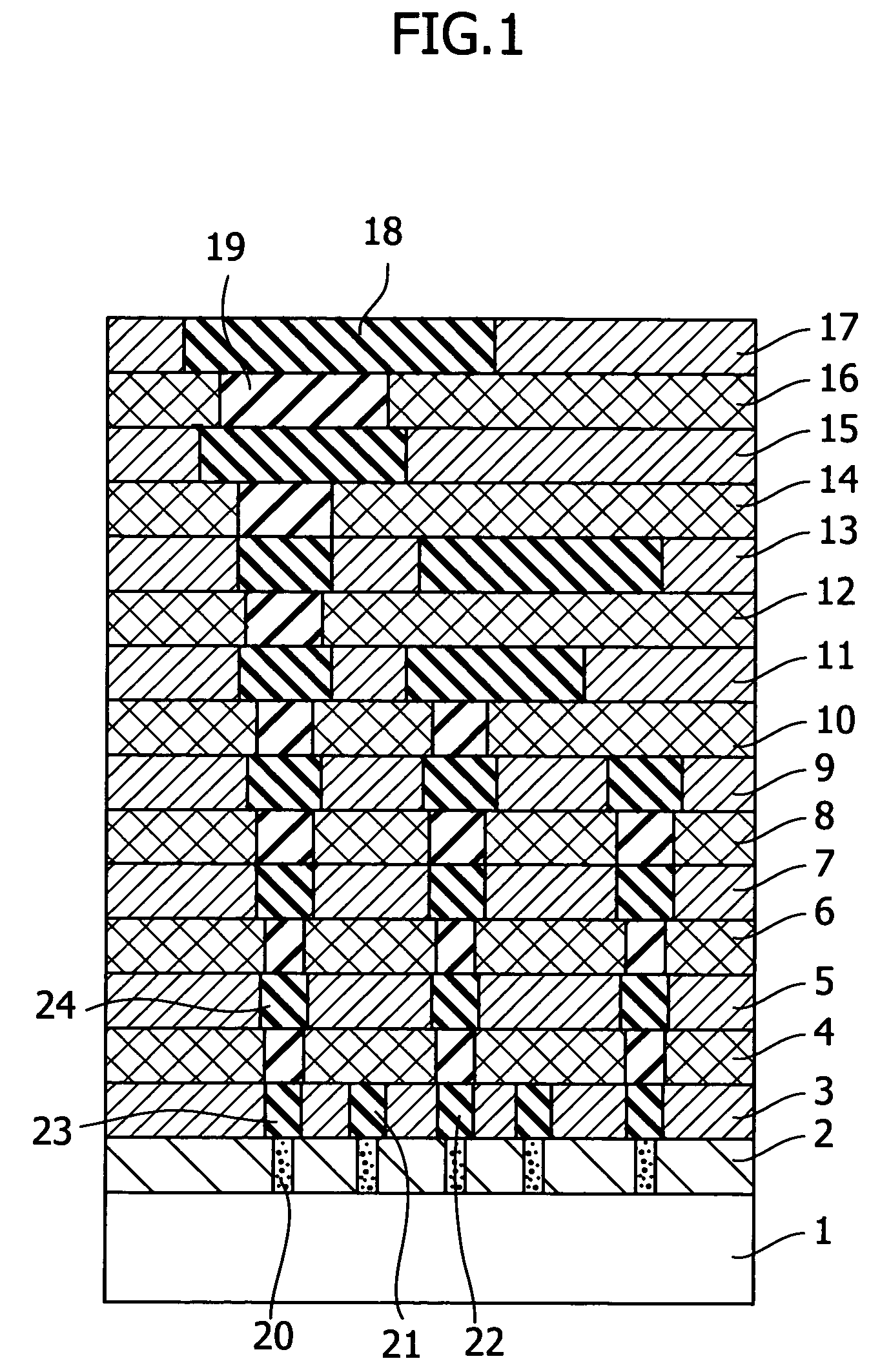
Image

Examples
example 1
[0071]The 178 g of ethanol and 95 g of an 1.68 wt % solution of tetramethylammonium hydroxide (made by Tama Chemicals Company) were uniformly mixed. After this solution was raised to 60° C., a mixture of 19.3 g methyltrimethoxysilane, 26.9 g tetraethoxysilane and 5 g tris(2-(trimethoxysilyl)ethyl)methylsilane was added dropwise thereto over two hours at this temperature. Then, the solution was stirred for two hours at 60° C., and 10.5 g of 20 wt % maleic acid and 165 g propylene glycol monopropyl ether were added thereto. The resulting solution was concentrated with a rotary evaporator until the solution became 160 g. The 150 g ethyl acetate and 150 g ultrapure water were added thereto, stirred, left to stand still, and separated to obtain an organic phase. The organic phase was concentrated again until the weight of the solution reached 150 g so as to yield a desired coating liquid. The coating liquid was applied on an 8-inch wafer with a spin coater at 1500 rpm for one minute. The...
example 2
[0073]The coating liquid was obtained in the same manner as in Example except that 95.8 g of an aqueous 2.23 wt % solution of choline (made by Tama Chemicals Company) was added in the place of the 1.68 wt % solution of tetramethylammonium hydroxide. The coated film was otained in the same manner as Example 1. The film had thickness of 5,800 A, dielectric constant of 2.3 and modulus of elasticity of 7.9 GPa.
example 3
[0074]The coating liquid was obtained in the same manner as in Example except that 97.5 g of an aqueous 3.78 wt % solution of tetrapropylammonium hydroxide (made by Tama Chemicals Company) was added in the palce of the 1.68 wt % solution of tetramethylammonium hydroxide. The coated film was obtained in the same manner as Example 1. The film had the thickness of 4,800 A, dielectric constant of 2.2 and modulus of elasticity of 5.9 GPa.
PUM
| Property | Measurement | Unit |
|---|---|---|
| Thickness | aaaaa | aaaaa |
| Dielectric polarization enthalpy | aaaaa | aaaaa |
| Composition | aaaaa | aaaaa |
Abstract
Description
Claims
Application Information
 - R&D
- Intellectual Property
- Life Sciences
- Materials
- Tech Scout
- Unparalleled Data Quality
- Higher Quality Content
- 60% Fewer Hallucinations
Browse by: Latest US Patents, China's latest patents, Technical Efficacy Thesaurus, Application Domain, Technology Topic, Popular Technical Reports.
© 2025 PatSnap. All rights reserved.Legal|Privacy policy|Modern Slavery Act Transparency Statement|Sitemap|About US| Contact US: help@patsnap.com