Semiconductor manufacturing apparatus and pattern formation method
a manufacturing apparatus and pattern technology, applied in the direction of photosensitive materials, instruments, printers, etc., can solve the problems of reducing the productivity and yield in the fabrication process of semiconductor devices, resist pattern defect, etc., to and reduce the thickness of the surface film
- Summary
- Abstract
- Description
- Claims
- Application Information
AI Technical Summary
Benefits of technology
Problems solved by technology
Method used
Image
Examples
embodiment 1
Modification of Embodiment 1
[0076]Now, a modification of Embodiment 1 will be described with reference to the accompanying drawing.
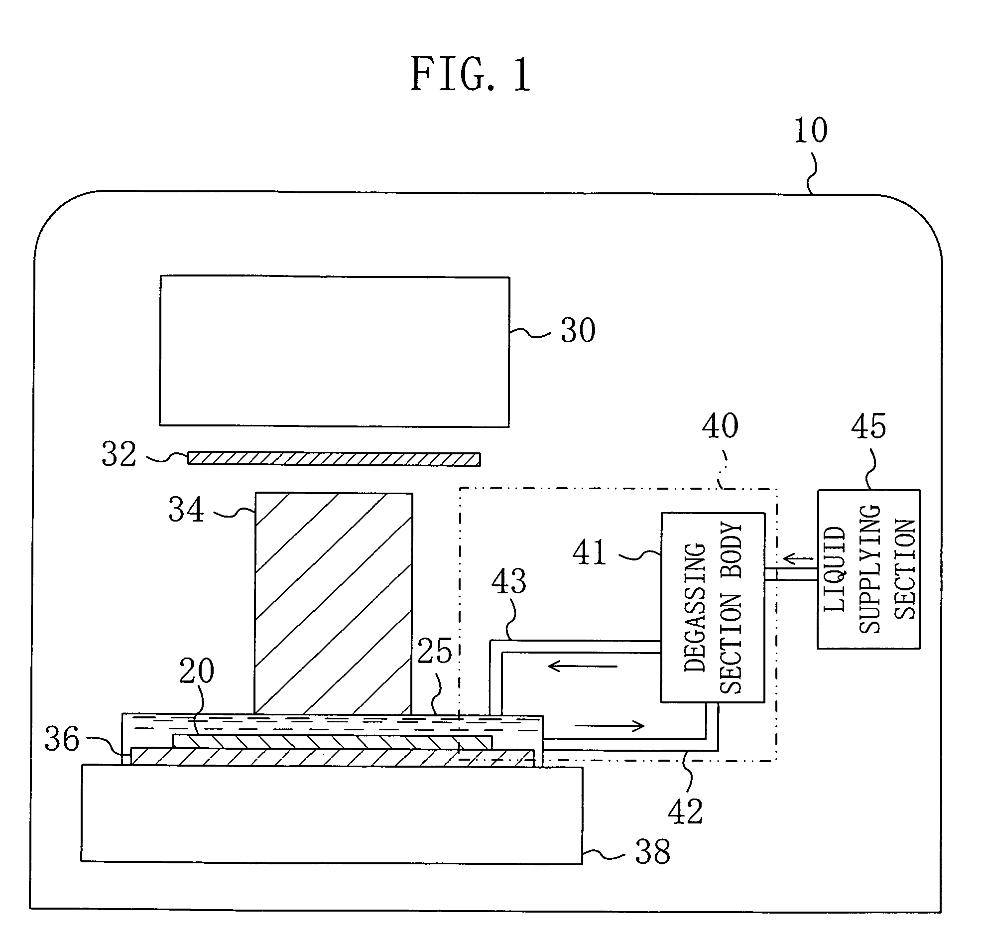
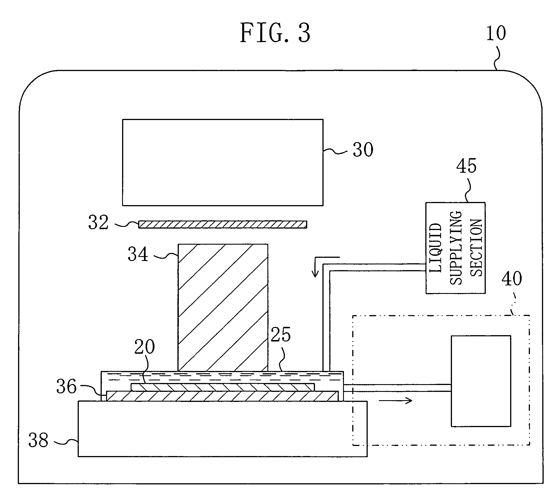
[0077]FIG. 3 schematically shows the cross-sectional structure of a principal part of a semiconductor manufacturing apparatus used for realizing a pattern formation method employing the immersion lithography according to the modification of Embodiment 1. In FIG. 3, like reference numerals are used to refer to like elements shown in FIG. 1 so as to omit the description.
[0078]As shown in FIG. 3, in the semiconductor manufacturing apparatus of this modification, a liquid 25 provided onto a wafer 20 is directly supplied from a liquid supplying section 45, and the liquid 25 having been provided onto the wafer 20 is degassed by a degassing section 40 during exposure. The liquid 25 supplied from the liquid supplying section 45 may or may not be previously degassed. Moreover, there is no need to always perform the degassing process but it may be appropriately pe...
embodiment 2
[0081]FIG. 4 schematically shows the cross-sectional structure of a principal part of a semiconductor manufacturing apparatus used for realizing a pattern formation method employing the immersion lithography according to Embodiment 2 of the invention. In FIG. 4, like reference numerals are used to refer to like elements shown in FIG. 1 so as to omit the description.
[0082]As shown in FIG. 4, in the semiconductor manufacturing apparatus of Embodiment 2, a liquid used for increasing the value of the numerical aperture of exposing light is partially provided onto the principal surface of a wafer 20, namely, provided in the form of drops, instead of employing the pooling method of Embodiment 1 and the modification in which the whole wafer 20 is immersed in the liquid.
[0083]In the dropping method of this embodiment, the liquid 25 in the form of drops is allowed to flow during the movement of the movable stage 36 at a flow rate for preventing the air from being swallowed up into the liquid...
embodiment 3
[0098]FIG. 6 schematically shows the cross-sectional structure of a principal part of an exposure system, that is, a semiconductor manufacturing apparatus, used for realizing a pattern formation method employing the immersion lithography according to Embodiment 3 of the invention.
[0099]As shown in FIG. 6, the exposure system of Embodiment 3 includes an illumination optical system 130 provided within a chamber 110 and working as a light source for exposing a design pattern onto a resist film (not shown) applied on a wafer 120; and a liquid supplying section 140 for supplying, onto the resist film of the wafer 120, an immersion liquid 121A used for increasing the value of the numerical aperture of exposing light in the exposure.
[0100]Below the illumination optical system 130, a projection lens 131 for projecting, onto the resist film through the liquid 121A, the exposing light emitted from the illumination optical system 130 and entering through a mask (reticle) 122 having a design pa...
PUM
| Property | Measurement | Unit |
|---|---|---|
| thickness | aaaaa | aaaaa |
| temperature | aaaaa | aaaaa |
| width | aaaaa | aaaaa |
Abstract
Description
Claims
Application Information
 - R&D
- Intellectual Property
- Life Sciences
- Materials
- Tech Scout
- Unparalleled Data Quality
- Higher Quality Content
- 60% Fewer Hallucinations
Browse by: Latest US Patents, China's latest patents, Technical Efficacy Thesaurus, Application Domain, Technology Topic, Popular Technical Reports.
© 2025 PatSnap. All rights reserved.Legal|Privacy policy|Modern Slavery Act Transparency Statement|Sitemap|About US| Contact US: help@patsnap.com


