Structure and method for fabricating semiconductor structures and devices for detecting an object
a semiconductor and object detection technology, applied in the direction of semiconductor laser structure details, semiconductor/solid-state device details, semiconductor laser details, etc., can solve the problems of low crystalline quality of monocrystalline materials and inability to fabricate semiconductor structures
- Summary
- Abstract
- Description
- Claims
- Application Information
AI Technical Summary
Problems solved by technology
Method used
Image
Examples
example 2
[0042]In accordance with a further embodiment of the invention, monocrystalline substrate 22 is a silicon substrate as described above. The accommodating buffer layer is a monocrystalline oxide of strontium or barium zirconate or hafnate in a cubic or orthorhombic phase with an amorphous intermediate layer of silicon oxide formed at the interface between the silicon substrate and the accommodating buffer layer. The accommodating buffer layer can have a thickness of about 2–100 nm and preferably has a thickness of at least 5 nm to ensure adequate crystalline and surface quality and is formed of a monocrystalline SrZrO3, BaZrO3, SrHfO3, BaSnO3 or BaHfO3. For example, a monocrystalline oxide layer of BaZrO3 can grow at a temperature of about 700 degrees C. The lattice structure of the resulting crystalline oxide exhibits a 45 degree rotation with respect to the substrate silicon lattice structure.
[0043]An accommodating buffer layer formed of these zirconate or hafnate materials is suit...
example 3
[0044]In accordance with a further embodiment of the invention, a structure is provided that is suitable for the growth of an epitaxial film of a monocrystalline material comprising a II–VI material overlying a silicon substrate. The substrate is preferably a silicon wafer as described above. A suitable accommodating buffer layer material is SrxBa1-xTiO3, where x ranges from 0 to 1, having a thickness of about 2–100 nm and preferably a thickness of about 5–15 nm. Where the monocrystalline layer comprises a compound semiconductor material, the II–VI compound semiconductor material can be, for example, zinc selenide (ZnSe) or zinc sulfur selenide (ZnSSe). A suitable template for this material system includes 1–10 monolayers of zinc-oxygen (Zn—O) followed by 1–2 monolayers of an excess of zinc followed by the selenidation of zinc on the surface. Alternatively, a template can be, for example, 1–10 monolayers of strontium-sulfur (Sr—S) followed by the ZnSeS.
example 4
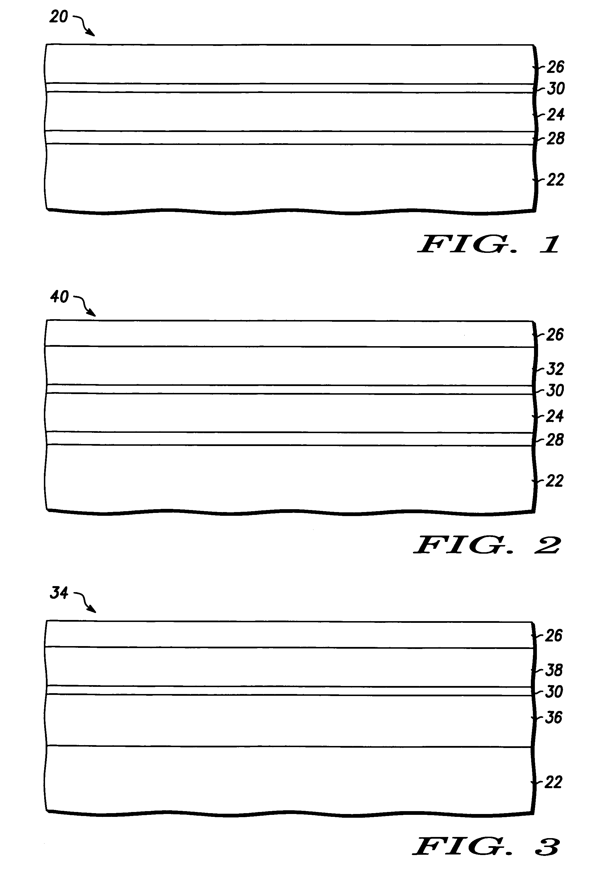
[0045]This embodiment of the invention is an example of structure 40 illustrated in FIG. 2. Substrate 22, accommodating buffer layer 24, and monocrystalline material layer 26 can be similar to those described in example 1. In addition, an additional buffer layer 32 serves to alleviate any strains that might result from a mismatch of the crystal lattice of the accommodating buffer layer and the lattice of the monocrystalline material. Buffer layer 32 can be a layer of germanium or a GaAs, an aluminum gallium arsenide (AlGaAs), an indium gallium phosphide (InGaP), an aluminum gallium phosphide (AlGaP), an indium gallium arsenide (InGaAs), an aluminum indium phosphide (AlInP), a gallium arsenide phosphide (GaAsP), or an indium gallium phosphide (InGaP) strain compensated superlattice. In accordance with one aspect of this embodiment, buffer layer 32 includes a GaAsxP1-x superlattice, wherein the value of x ranges from 0 to 1. In accordance with another aspect, buffer layer 32 includes ...
PUM
 Abstract
Description
Claims
Application Information
 - R&D
- Intellectual Property
- Life Sciences
- Materials
- Tech Scout
- Unparalleled Data Quality
- Higher Quality Content
- 60% Fewer Hallucinations
Browse by: Latest US Patents, China's latest patents, Technical Efficacy Thesaurus, Application Domain, Technology Topic, Popular Technical Reports.
© 2025 PatSnap. All rights reserved.Legal|Privacy policy|Modern Slavery Act Transparency Statement|Sitemap|About US| Contact US: help@patsnap.com


