
Decreasing metal-silicide oxidation during wafer queue time

a technology of metalsilicide and wafers, applied in semiconductor devices, semiconductor/solid-state device details, electrical devices, etc., can solve the problems of wafers “in queue", exposed portions begin to oxidize, and the trend of ever smaller and denser devices is over

Inactive Publication Date: 2007-01-09
TAIWAN SEMICON MFG CO LTD
View PDF3 Cites 7 Cited by
  • Summary
  • Abstract
  • Description
  • Claims
  • Application Information

AI Technical Summary

Benefits of technology

[0006]Thus, if metal silicide pads have been formed but that wafer is put in queue while the metal silicide portions are exposed, those exposed portions begin to oxidize. Of course, the longer the wafer(s) stays in queue awaiting the next step in the manufacturing process, the more oxidation of the silicide takes place. Then, when the awaiting wafer finally reaches the point in the process where the metal interconnects (i.e., metal “plugs”) are formed in contact with silicide pads, the oxidized surfaces of the silicide pads detrimentally affect this electrical connection. Specifically, both the contact resistance and sheet resistance of the metal silicide pads are impacted, which results in reduced stability in the electrical connections, and thus a reduction in device performance. Accordingly, what is needed is a technique for reducing or eliminating the oxidation of exposed metal silicide in semiconductor wafers when those wafers are held in queue during the manufacturing process.

Problems solved by technology

Thus, semiconductor device improvements have been largely accomplished by reducing device feature size to the point where currently micron and sub-micron device features are being used, and predictions for future device sizes do not foresee an end to the trend of ever smaller and denser devices.
Since semiconductor wafers are typically mass-produced, delays in the manufacturing process often leave wafers “in queue,” awaiting the next step of the manufacturing process, and queue times of several days are not uncommon.
Thus, if metal silicide pads have been formed but that wafer is put in queue while the metal silicide portions are exposed, those exposed portions begin to oxidize.
Then, when the awaiting wafer finally reaches the point in the process where the metal interconnects (i.e., metal “plugs”) are formed in contact with silicide pads, the oxidized surfaces of the silicide pads detrimentally affect this electrical connection.
Specifically, both the contact resistance and sheet resistance of the metal silicide pads are impacted, which results in reduced stability in the electrical connections, and thus a reduction in device performance.

Method used


Image

  • Decreasing metal-silicide oxidation during wafer queue time
  • Decreasing metal-silicide oxidation during wafer queue time
  • Decreasing metal-silicide oxidation during wafer queue time

Examples


Embodiment Construction

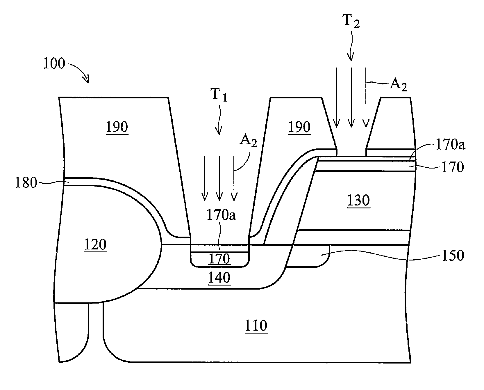
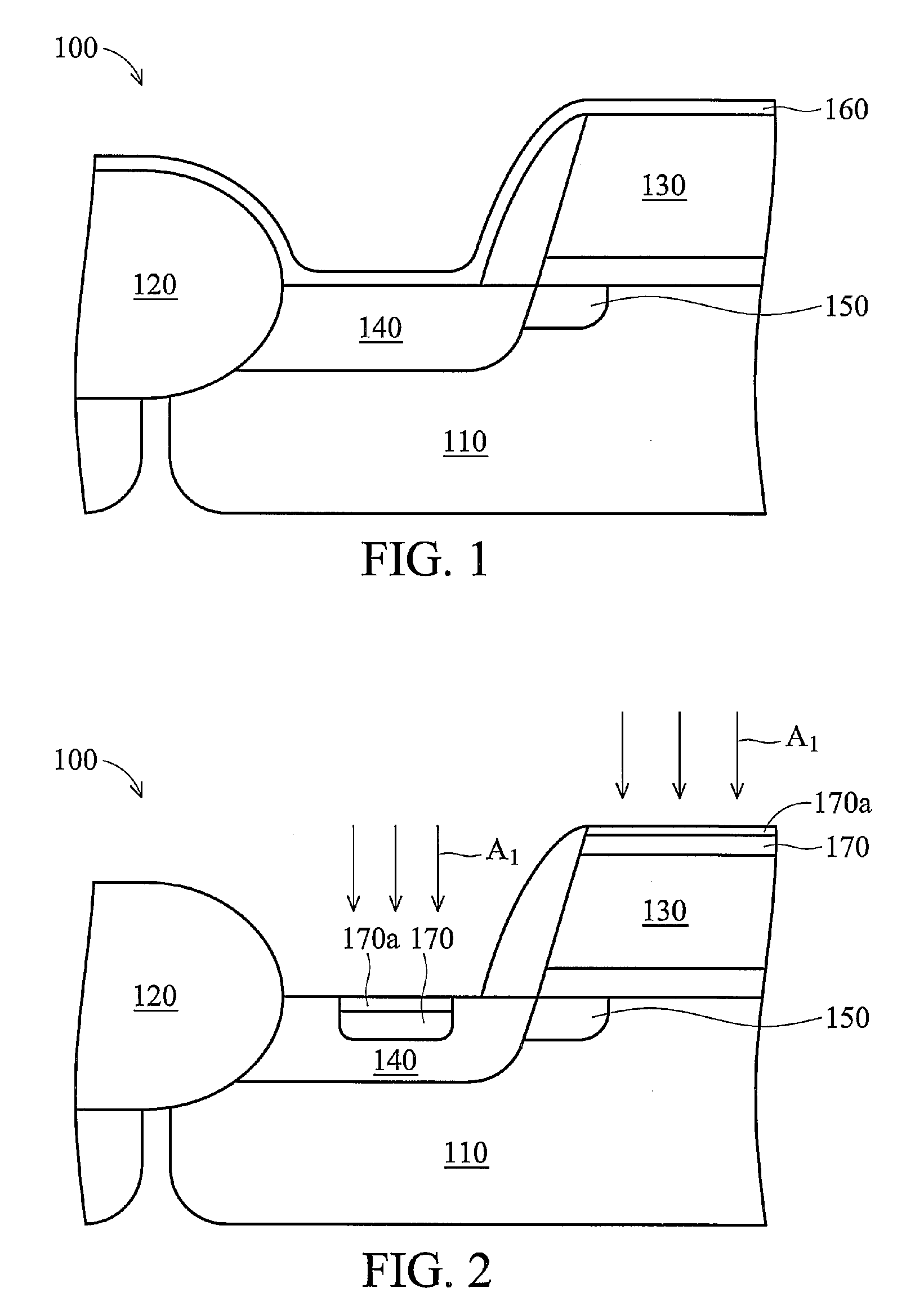
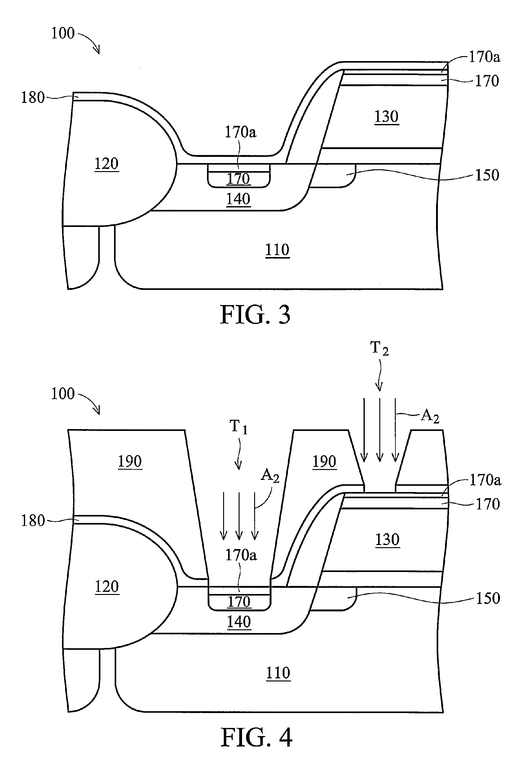
[0017]Referring initially to FIG. 1, illustrated is one embodiment of a semiconductor device 100 constructed according to the principles disclosed herein. The semiconductor device 100 is formed on a semiconductor substrate 110, which may be constructed from bulk silicon, silicon germanium, or may be a silicon-on-insulator (SOI) substrate. Separating active regions on the substrate 110 are field oxides 120 (only one is illustrated), which may be formed using conventional techniques.

[0018]In the illustrated embodiment of FIG. 1, the semiconductor device 100 is a metal-oxide-semiconductor (MOS) transistor device 100, which includes a gate electrode 130 formed on the substrate 110. The gate electrode 130 may be formed using polysilicon as in conventional techniques, however, other materials may also be employed. Also constructed as part of the MOS transistor device 100 are a source / drain region 140 and a lightly-doped drain (LDD) region 150. Both of these components of the device 100 ma...


PUM

PropertyMeasurementUnit
temperatureaaaaaaaaaa
pressureaaaaaaaaaa
feature sizeaaaaaaaaaa

Abstract

Disclosed herein are various embodiments of semiconductor devices and related methods of manufacturing a semiconductor device. In one embodiment, a method includes providing a semiconductor substrate and forming a metal silicide on the semiconductor substrate. In addition, the method includes treating an exposed surface of the metal silicide with a hydrogen / nitrogen-containing compound to form a treated layer on the exposed surface, where the composition of the treated layer hinders oxidation of the exposed surface. The method may then further include depositing a dielectric layer over the treated layer and the exposed surface of the metal silicide.

Description

TECHNICAL FIELD [0001]Disclosed embodiments herein relate generally to the manufacture of semiconductor devices, and more particularly to semiconductor devices and related methods of manufacturing have decreased oxidation on metal silicide components while the semiconductor wafer is in queue awaiting the next processing step.BACKGROUND[0002]As technology in products and equipment continue to become more complex, the use of integrated circuit (IC) devices in these products and equipment is basically essential. In addition, consumers and manufacturers alike have continued to desire smaller product size, which requires a continued decrease in overall IC chip size. As a result, the large-scale integration of circuit components, such as transistors and capacitors, has become a necessity for decreased overall size, but increased device performance. Thus, semiconductor device improvements have been largely accomplished by reducing device feature size to the point where currently micron and...

Claims


Application Information

Patent Timeline
Patent Type & Authority Patents(United States)
IPC IPC(8): H01L21/4763H01L23/48
CPCH01L21/3003H01L29/665H01L21/76888
Inventor WU, ZHEN-CHENGCHANG, CHENG-HUNGHUANG, YU-LIENCHENG, SHWANG-MING
Owner TAIWAN SEMICON MFG CO LTD
Learn More