
Lamination and delamination technique for thin film processing

a thin film and delamination technology, applied in the direction of diffusion transfer process, pulse technique, instruments, etc., can solve the problems of high water absorption, less than ideal thermal and mechanical properties, high cost, etc., and achieve excellent mechanical stability and good adhesion

Inactive Publication Date: 2006-11-28
TERECIRCUITS CORP +1
View PDF13 Cites 35 Cited by
  • Summary
  • Abstract
  • Description
  • Claims
  • Application Information

AI Technical Summary

Benefits of technology

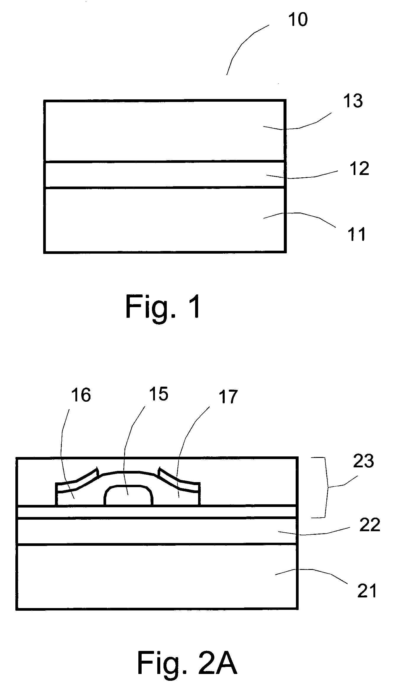
[0011]This invention provides a lamination-transfer, or lamination-delamination, process employing a releasable adhesion layer having good adhesion and excellent mechanical stability during high temperature fabrication processes of thin film devices in the absence of light, and delaminating at a lower temperature in the presence of light for transferring to a target substrate.

Problems solved by technology

500° C. However, quartz and heat resistant glass substrates are expensive, heavy and fragile.
But these polymer substrates are often colored, very expensive, have high water absorbance and less than ideal thermal and mechanical properties.
It has been extremely difficult to satisfy both these required process conditions and desirable product characteristics.
However, the most difficult aspect of the substrate transfer method is the selection of the releasable adhesion layer.
Currently to the best of our knowledge, there is no suitable releasable adhesion layer, one that can provide good adhesion during high temperature fabrication processing and at the same time can delaminate at a low temperature for transferring to a target substrate.

Method used


Image

  • Lamination and delamination technique for thin film processing
  • Lamination and delamination technique for thin film processing
  • Lamination and delamination technique for thin film processing

Examples


Embodiment Construction

[0029]The present invention lamination-transfer, or lamination-delamination, or simply transfer process offers a solution to the mismatching substrate problem between the requirements of a substrate for fabrication processes and the characteristics desirable for a product substrate.

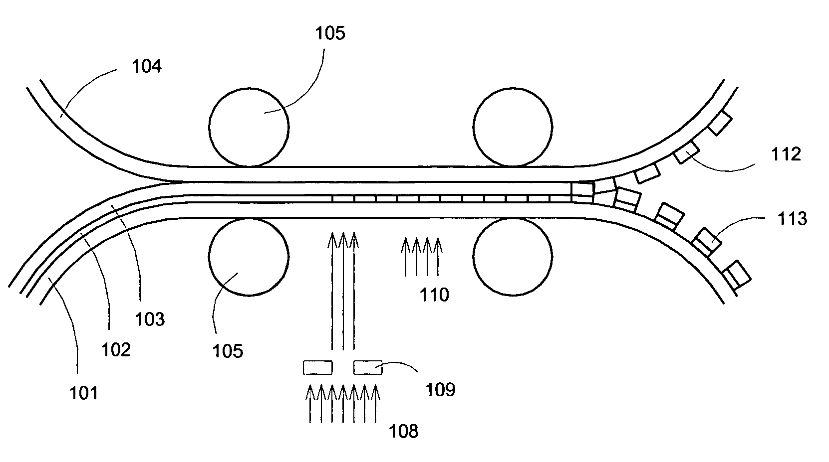
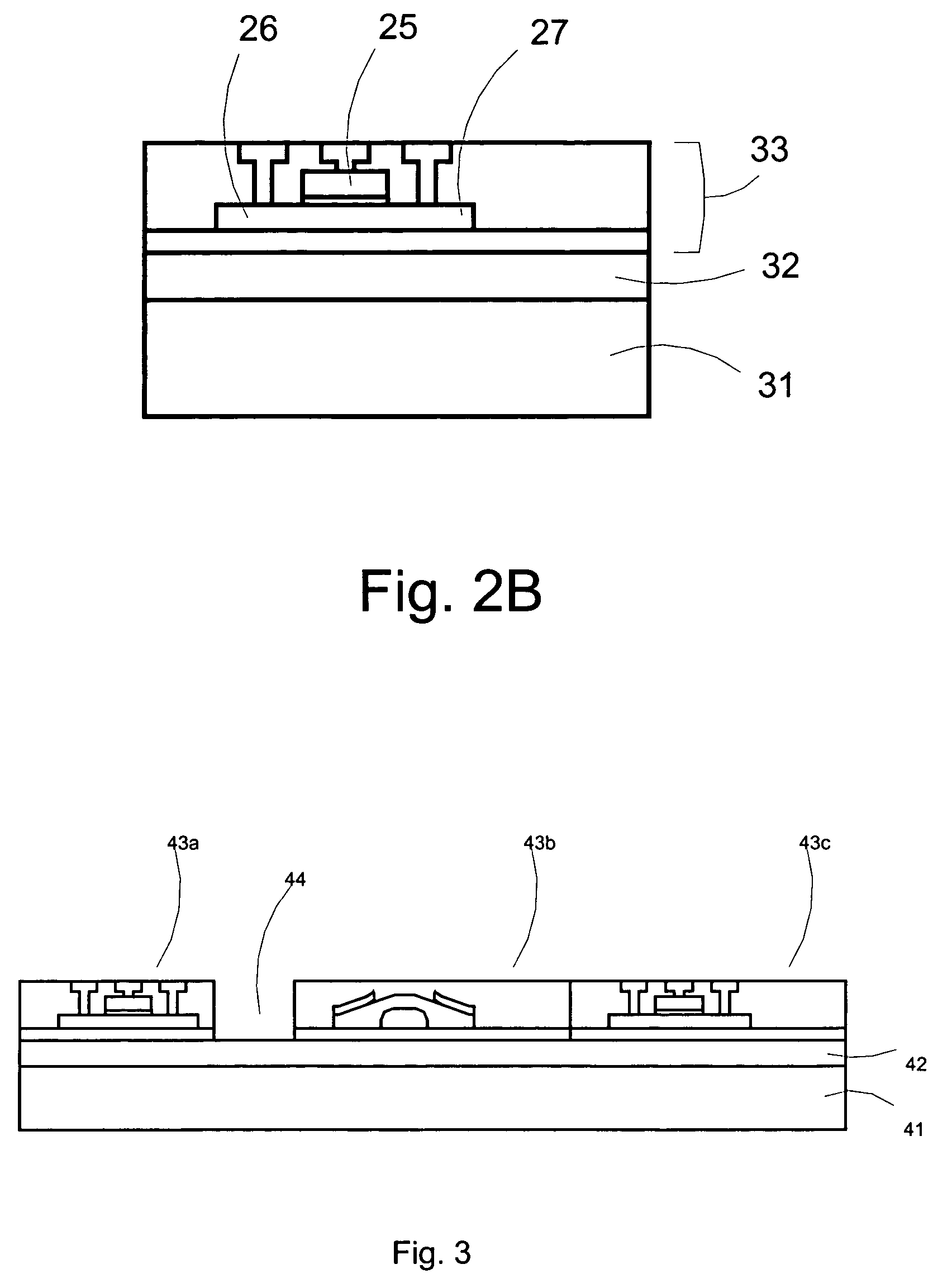
[0030]The disclosed transfer process involves the following steps: Semiconducting or other thin film devices with fine patterns are fabricated on a substrate with the desired optimal properties for fabrication that has been first coated with a suitable releasable adhesion layer. Subsequently, a second substrate with the desired properties for the target use of the fabricated semiconductor device is laminated onto the top of the devices. A trigger process is used to separate the devices from the fabrication substrate resulting in the semiconductor devices being attached to the second substrate. This process may be used with either finished devices (typically multilayer in construction), or with individual ...


PUM

PropertyMeasurementUnit
heat resistanceaaaaaaaaaa
temperaturesaaaaaaaaaa

Abstract

This invention discloses a releasable adhesion layer having good adhesion during high temperature fabrication process in the absence of light, and delaminating at a lower temperature in the presence of light. One embodiment of this invention is a film of polymer whose thermal decomposition temperature changes drastically upon photoexposure. These materials, prior to photoexposure, can withstand temperatures in the range of approximately 200° C. to 300° C. without decomposition, yet decompose at around 100° C. with photoexposure. The releasable adhesion layer can be used in a thermal transfer element, sandwiching a donor substrate and a transfer layer having a plurality of multicomponent transfer units. In the absence of light, the releasable adhesion layer can sustain high temperature processing of these multicomponent transfer units. By photoexposing according to a pattern, the photoexposed multicomponent transfer units can be selectively released at a low temperature to transfer to a receptor.

Description

FIELD OF THE INVENTION[0001]This invention relates to thin film device transfer elements and methods of transferring thin film devices to a receptor. In particular, the invention relates to the problem of producing devices on substrates whose thermal, mechanical or optical properties may be incompatible with the processing conditions necessary to fabricate such devices.BACKGROUND OF THE INVENTION[0002]In the manufacturing of thin film device products, thin film devices such as field effect transistors (FET), thin film transistors (TFT), light emitting diodes (LED), memory circuits, display circuits or optical devices are fabricated on a substrate through various processes such as chemical vapor deposition, etching, oxidation, and annealing. Since the fabrication processes often involve high temperature treatment, one of the substrate requirements is high temperature heat resistance, meaning the substrate must have a high softening temperature and a high melting temperature. To minim...

Claims


Application Information

Patent Timeline
Patent Type & Authority Patents(United States)
IPC IPC(8): G03F7/34B41M5/382H01L31/153H01L51/40
CPCB41M5/38214H01L51/0013H01L51/0024G03F7/34H10K71/18H10K71/50
Inventor SHEATS, JAMESNGUYEN, TUE
Owner TERECIRCUITS CORP
Learn More