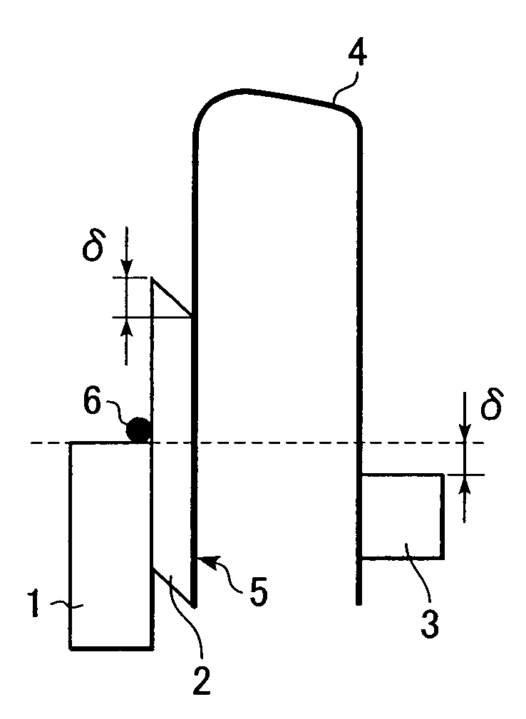
Electron emission device, electron source, and image display having dipole layer
an electron emission device and electron source technology, applied in the direction of instruments, discharge tubes, luminescnet screens, etc., can solve the problems of degrading displayed images or the contrast of images, delaying the control, and emitted electrons, etc., to achieve efficient electron emission, high contrast, and easy emission
- Summary
- Abstract
- Description
- Claims
- Application Information
AI Technical Summary
Benefits of technology
Problems solved by technology
Method used
Image
Examples
example 1
[0117]According to the manufacturing method shown in FIG. 10, a semiconductor layer (an electron-emission layer) having a dipole layer according to the present invention was manufactured. References in FIG. 10 are identical to those in FIG. 7.
[0118]Using quartz as the substrate 31, a TiN film with a thickness of 500 nm was formed by sputtering as the cathode electrode 1 after the substrate 31 was sufficiently washed (FIG. 10A). The film forming conditions are as follows:[0119]Rf power supply: 13.56 MHz[0120]Rf power: 7.7 W / cm2 [0121]gas pressure: 0.6 Pa[0122]atmosphere gas: N2 / Ar (N2:10%)[0123]substrate temperature: room temperature[0124]target: Ti
[0125]Then, a carbon film was deposited with a thickness of 4 nm on the cathode electrode 1 by sputtering so as to form the insulation layer 2 (FIG. 10B). Using a graphite target as the target, the film was formed in an argon atmosphere.
[0126]Next, the above-mentioned insulation layer 2 was heat-treated in a mixed gas atmosphere of methane...
example 2
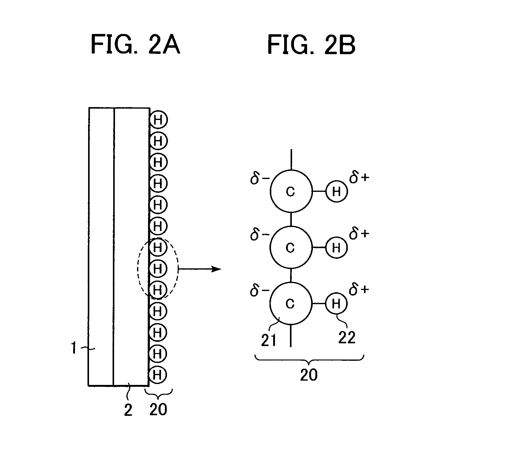
[0139]According to the manufacturing method shown in FIG. 10, an insulation layer 2 having a dipole layer 20 according to the present invention was manufactured.
[0140]Using quartz as the substrate 31, a W film with a thickness of 500 nm was formed by sputtering as the cathode electrode 1 after the substrate 31 was sufficiently washed (FIG. 10A).
[0141]Then, SiO2 was deposited with a thickness of about 4 nm on the cathode electrode 1 by sputtering so as to form the insulation layer 2 (FIG. 10B). Mixed gas of Ar / O2=1 / 1 was used for an atmosphere gas. The conditions are as follows:[0142]Rf power supply: 13.56 MHz[0143]Rf power: 110 W / cm2 [0144]gas pressure: 0.5 Pa[0145]substrate temperature: 300° C.[0146]target: SiO2
[0147]Next, the substrate was heat-treated in a mixed gas atmosphere of methane and hydrogen so as to form the dipole layer 20 on the surface (or at the surface) of the insulation layer 2 (FIG. 10C). The heat treatment conditions are as follows:[0148]heat treatment temperat...
example 3
[0154]According to the manufacturing method shown in FIG. 7, an electron emission device of the invention was manufactured.
(Process 1)
[0155]Using quartz as the substrate 31, a TiN film with a thickness of 500 nm was formed by sputtering as the electrode layer 71 after the substrate 31 was sufficiently washed.
(Process 2)
[0156]Then, a carbon film was deposited with a thickness of about 6 nm by ECR plasma CVD (electron cyclotron resonance plasma chemical vapor deposition) so as to form a semiconductor layer 2 (FIG. 7A). This was under conditions that the DLC (diamond-like carbon) grows. The growing conditions are as follows:[0157]gas: CH4 [0158]microwave power: 400 W[0159]substrate bias: −90 V[0160]gas pressure: 25 mm Pa[0161]substrate temperature: room temperature
(Process 3)
[0162]Next, as shown in FIG. 7B, a positive-type photoresist (AZ® 1500 made by Clariant Co.) was spin-coated, exposed, and developed by photolithography so as to form a mask pattern (the photoresist 72).
(Process 4)...
PUM
 Abstract
Description
Claims
Application Information
 - R&D
- Intellectual Property
- Life Sciences
- Materials
- Tech Scout
- Unparalleled Data Quality
- Higher Quality Content
- 60% Fewer Hallucinations
Browse by: Latest US Patents, China's latest patents, Technical Efficacy Thesaurus, Application Domain, Technology Topic, Popular Technical Reports.
© 2025 PatSnap. All rights reserved.Legal|Privacy policy|Modern Slavery Act Transparency Statement|Sitemap|About US| Contact US: help@patsnap.com


