
Methods of producing integrated circuit devices utilizing tantalum amine derivatives

a technology of tantalum amine and derivatives, applied in the direction of coatings, transistors, chemical vapor deposition coatings, etc., can solve the problems of degrading the characteristics of the semiconductor device, additional damage to the electrode, and limited thickness reduction of silicon oxide layers used as gate insulating layers

Inactive Publication Date: 2006-07-25
SAMSUNG ELECTRONICS CO LTD
View PDF20 Cites 50 Cited by
  • Summary
  • Abstract
  • Description
  • Claims
  • Application Information

AI Technical Summary

Benefits of technology

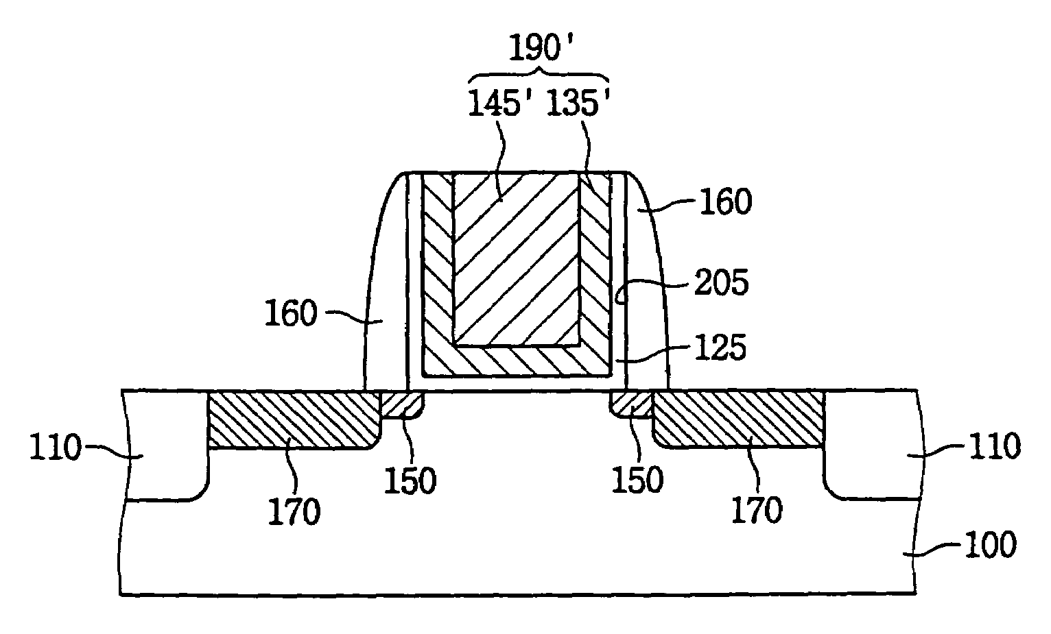
[0024]In a method for forming a gate electrode in accordance with one aspect of the present invention, a dielectric layer having a high dielectric constant is formed on a substrate. Tantalum amine derivatives represented by a chemical formula Ta(NR1)(NR2R3)3 wherein R1, R2 and R3 represent H or C1–C6 alkyl group are introduced onto the dielectric layer to form a metal barrier layer. A gate metal layer is formed on the metal barrier layer. The gate metal layer and the metal barrier layer are patterned to form a gate metal pattern and a metal barrier pattern. The tantalum amine derivative may introduced into at a temperature of about 100° C. to about 650° C. The metal layer may be deposited by a chemical vapor deposition (CVD) process, a plasma enhanced CVD (PECVD) process, an atomic layer deposition (ALD) process, and a radical assisted ALD (RAALD) process. The dielectric layer may include tantalum oxide (Ta2O5), titanium oxide (TiO2), hafnium o

Problems solved by technology

When the thickness of the gate insulating layer is reduced to less than a critical thickness, a leakage current may occur thereby degrading characteristics of the semiconductor device.
Thus, further reduction in thickness of silicon oxide layers used as gate insulating layers may be limited.
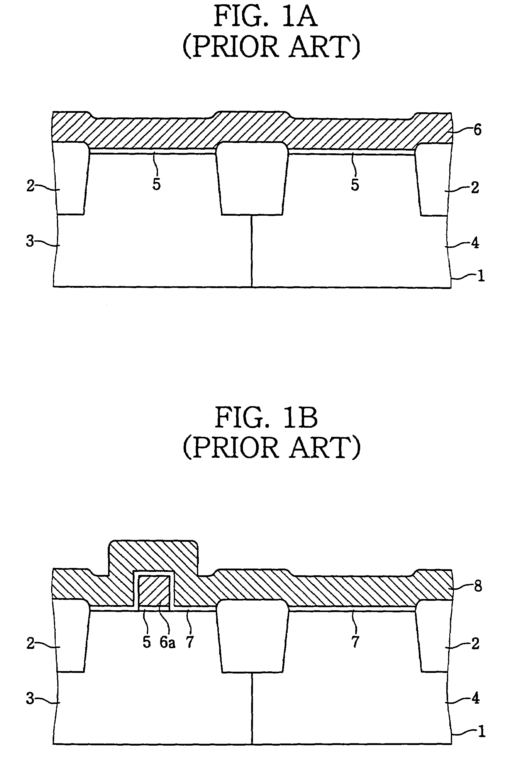
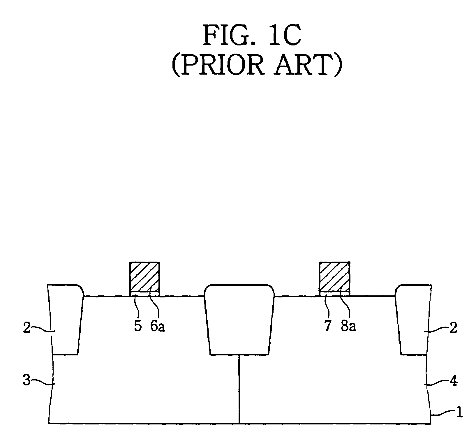
Furthermore, the method for manufacturing the N-MOS gate electrode 6a and the P-MOS gate electrode 8a using a damascene process may cause additional damage to the electrodes.
Oxygen contained in a metal oxide material may be readily reacted with silicon and may cause the deterioration of the characteristics of the capacitor.
This, in turn, may result in a reduction in the reliability of an integrated circuit.

Method used


Image

  • Methods of producing integrated circuit devices utilizing tantalum amine derivatives
  • Methods of producing integrated circuit devices utilizing tantalum amine derivatives
  • Methods of producing integrated circuit devices utilizing tantalum amine derivatives

Examples


examples

[0156]Gate electrodes were formed using various methods including the method of the present invention. Work functions of the gate electrodes were measured. The measured work functions were showed in following Table 1. In Table 1, I→A represented inversion→accumulation. A→I represented accumulation→inversion. Delta indicated a difference between I→A and A→I. Delta had originally a substantially same value. However, delta had a different value according to a direction of applied voltage due to an oxide trap charge. This was called as hysteresis. The work functions were measured from I→A or A→I. A standard work function of TiN was 4.7 eV. A standard work function of poly was 4.1 eV.

[0157]

TABLE 1ElectrodeI→AA→IDeltaWork functionP-TiN (Ti-rich)−0.36−0.33304.75P-TiN (N-rich)−0.42−0.331104.69P-TaN (Ta-rich)−0.8−0.78204.31P-TaN (N-rich)−0.72−0.73104.39P-Ta−0.79−0.7904.32A-TaN of 100 Å−0.62−0.6204.49A-TaN of 200 Å−0.66−0.67104.45C-TaN of 200 Å−0.34−0.35104.77A-TaN of 400 Å−0.85−0.83204.26Pol...


PUM

PropertyMeasurementUnit
Temperatureaaaaaaaaaa
Pressureaaaaaaaaaa

Abstract

In a method for forming a gate electrode, a dielectric layer having a high dielectric constant is formed on a substrate. Tantalum amine derivatives represented by a chemical formula Ta(NR1)(NR2R3)3 in which R1, R2 and R3 represent H or C1–C6 alkyl group are introduced onto the dielectric layer to form a tantalum nitride layer. A capacitor metal layer or a gate metal layer is formed on the tantalum nitride layer. The capacitor metal layer or the gate metal layer and the tantalum nitride layer are patterned to form a capacitor electrode or a gate electrode. The tantalum amine derivatives are used in forming a dual gate electrode.

Description

CROSS REFERENCE TO RELATED APPLICATIONS[0001]This application is a Continuation-In-Part of U.S. patent application Ser. No. 10 / 196,814, filed on Jul. 17, 2002 now abandoned; U.S. patent application Ser. No. 10 / 408,631, filed on Apr. 7, 2003 now abandoned; U.S. patent application Ser. No. 10 / 411,949, filed on Apr. 11, 2003 now abandoned; and U.S. patent application Ser. No. 10 / 425,276, filed on Apr. 29, 2003, now U.S. Pat. No. 6,815,285, the contents of which are herein incorporated by reference in its entirety as if set forth fully herein. This application also claims priority under 35 USC § 119 to Korean Patent Application No. 2003-42844, filed on Jun. 27, 2003, the contents of which are herein incorporated by reference in its entirety as if set forth fully herein.BACKGROUND OF THE INVENTION[0002]1. Field of the Invention[0003]The present invention relates to methods of forming an electrode for an integrated circuit device.[0004]2. Description of the Related Art[0005]A transistor o...

Claims


Application Information

Patent Timeline
IPC IPC(8): H01L21/44H01L21/28H01L21/336H01L21/8234H01L21/8238H01L29/49H01L29/51H01L29/78
CPCC23C16/34H01L29/7833H01L21/265H01L21/28088H01L21/28194H01L21/823425H01L21/823842H01L29/4966H01L29/517H01L29/6656H01L29/66583H01L29/6659C23C16/56H01L21/28556H01L21/76841
Inventor KANG, SANG-BOMLEE, JONG-MYEONGCHOI, KYUNG-INCHOI, GIL-HEYUNLEE, YOU-KYOUNGPARK, SEONG-GEONLEE, SANG-WOO
Owner SAMSUNG ELECTRONICS CO LTD
Learn More