
Semiconductor protection device

a protection device and semiconductor technology, applied in the direction of transistors, pulse techniques, electronic switching, etc., can solve the problems of inability to obtain sufficient protection circuits, increase the cost of semiconductor devices, and increase the area of semiconductor devices, so as to avoid deterioration, increase the cost of semiconductor devices, and avoid deterioration

Inactive Publication Date: 2006-05-16
RENESAS TECH CORP
View PDF10 Cites 7 Cited by
  • Summary
  • Abstract
  • Description
  • Claims
  • Application Information

AI Technical Summary

Benefits of technology

[0005]An object of the invention is to provide a technique capable of improving destruction tolerance of a semiconductor device.
[0006]Another object of the invention is to provide a technique capable of reducing heat resistance of a semiconductor device.

Problems solved by technology

The inventors herein found that, although it is effective to electrically connect a protection circuit for clamping voltage to an output (that is, the collector side) of an amplifier constructed by HBTs to avoid deterioration and destruction of an HBT due to load fluctuation, when the protection circuit is simply attached, problems occur such that the chip area is enlarged, the cost of a semiconductor device increases, and a sufficient effect of the protection circuit cannot be obtained.
The proportion of the area occupied by the protection circuit in the whole semiconductor chip increases and a problem arise such that the cost of the semiconductor device increases.
As a result, it causes a problem such that the effect of the protection circuit is lost.
However, when the substrate is thinned, mechanical strength cannot be maintained and a problem of breakage of the substrate arises.
When the pitch of neighboring HBTs is decreased, a problem of increase in the chip size occurs.

Method used


Image

  • Semiconductor protection device
  • Semiconductor protection device
  • Semiconductor protection device

Examples


first embodiment

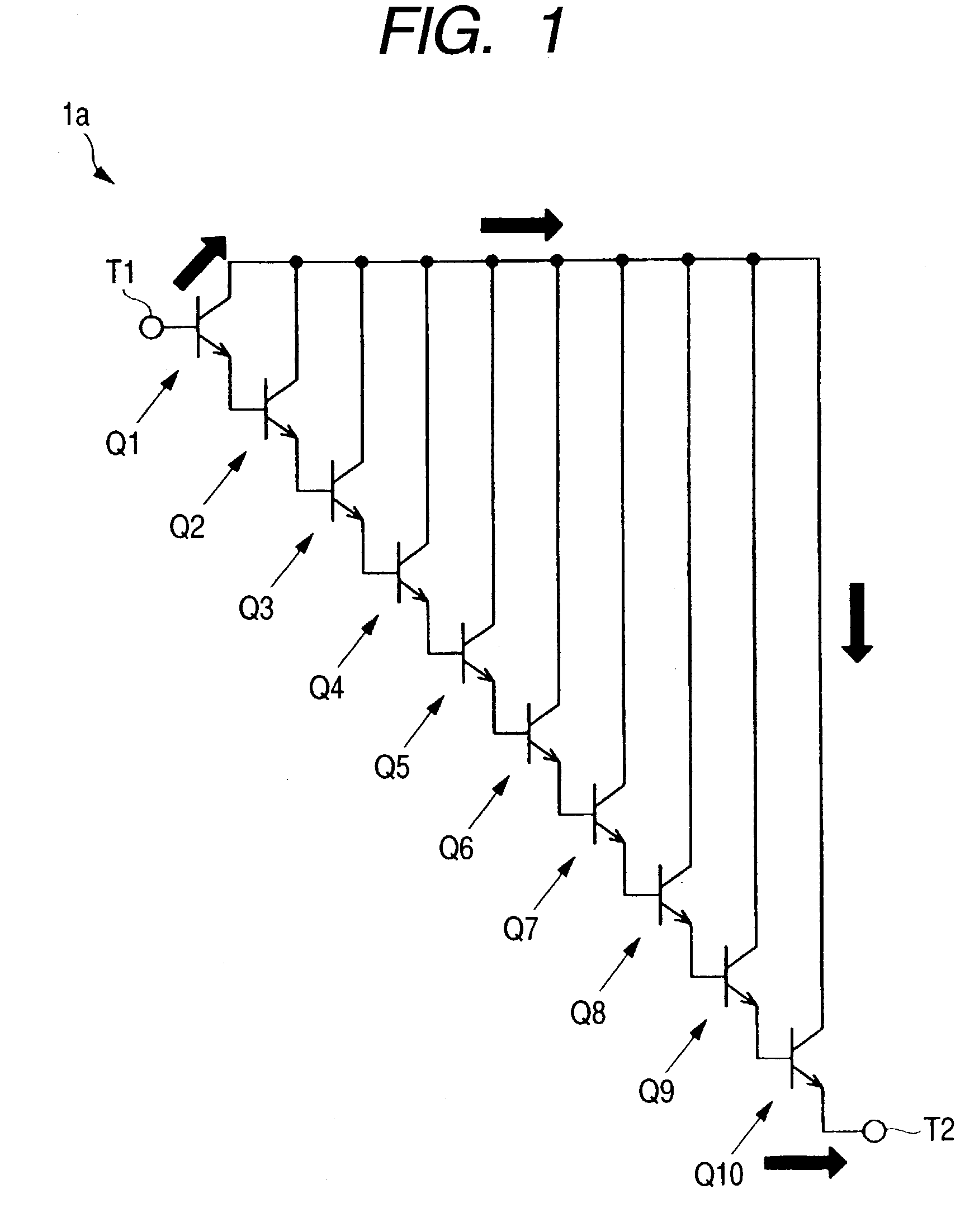
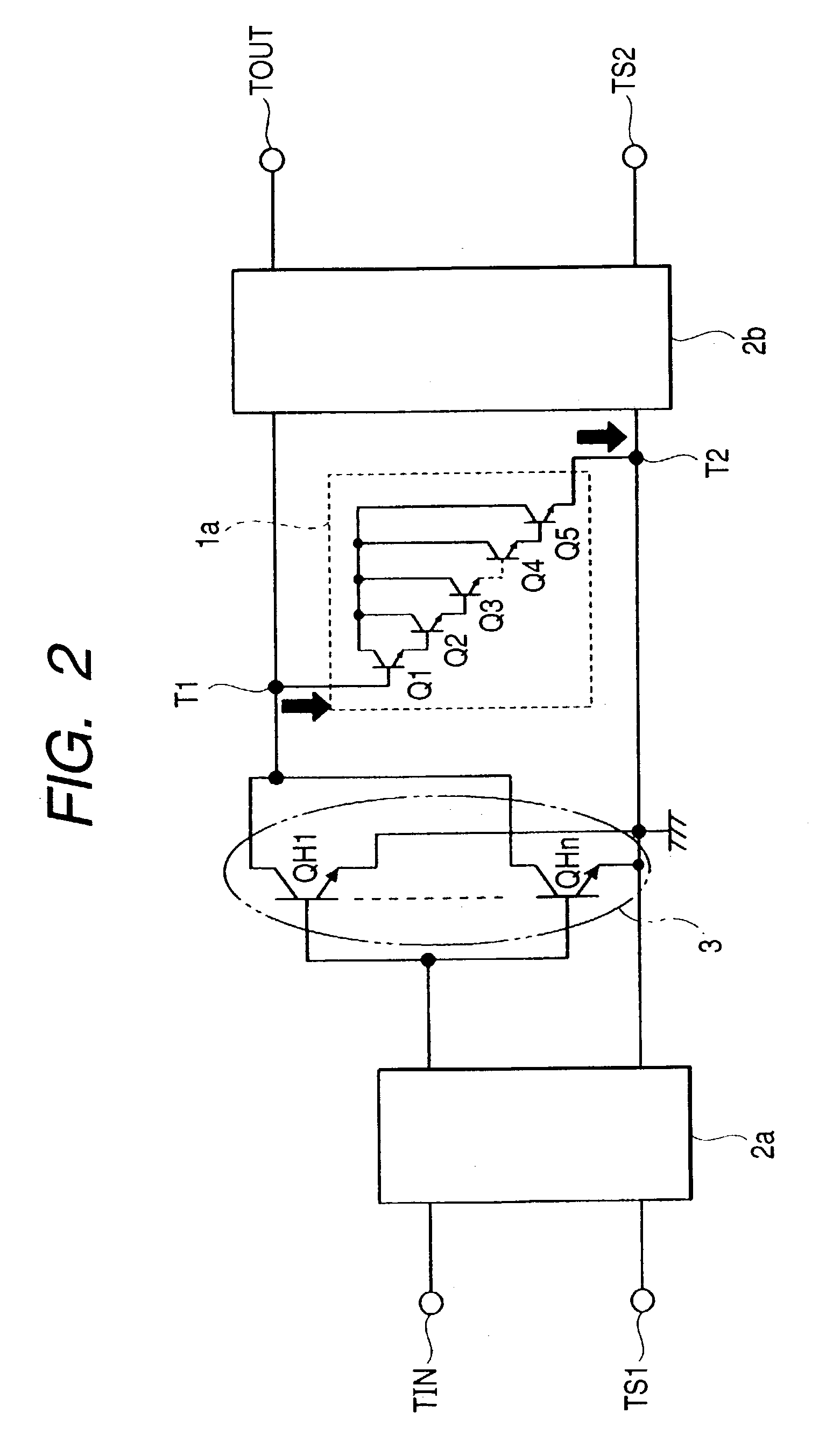
[0077]The inventors herein studied and, during development of a high-output amplifier for a radio communication device such as a vehicle telephone or portable telephone, found a phenomenon such that when a load impedance fluctuation test is conducted, an HBT (Heterojunction Bipolar Transistor) as a component of the high-output amplifier deteriorates or is destroyed. The phenomenon was analyzed and a result of the analysis that the HBT deteriorates or is destroyed since a high voltage is applied to the HBT temporarily. The load impedance fluctuation test is a test of measuring an influence on an internal circuit, which is exerted when the load of the amplifier is fluctuated.

[0078]In the first embodiment, therefore, by electrically connecting a protection circuit (protection device) for clamping voltage in a forward direction, a reverse direction, or in both of the forward and reverse directions to an output of the amplifier constructed by HBTs, that is, between the collector and emit...

second embodiment

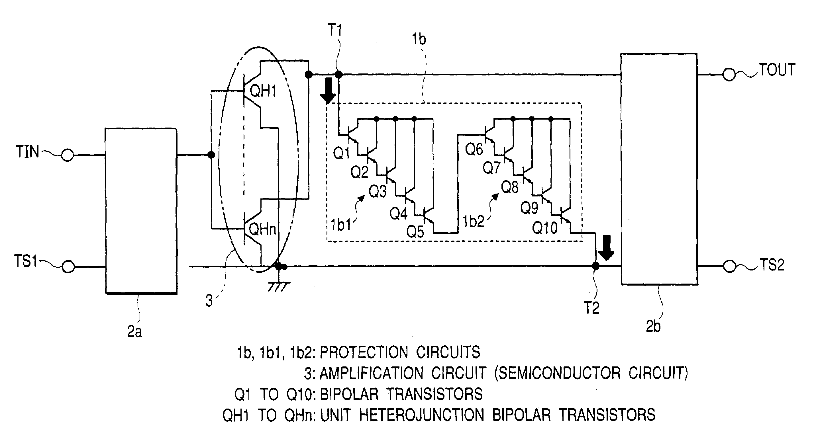
[0087]In a second embodiment, the protection circuit is divided into a plurality of blocks, and a group of a plurality of bipolar transistors which are Darlington connected is provided for each block.

[0088]FIG. 5 shows an example of a protection circuit 1b of the second embodiment. In the second embodiment as well, the protection circuit 1b has the ten bipolar transistors Q1 to Q10. In the second embodiment, the protection circuit 1b is divided into, for example, first and second blocks of two protection circuits 1b1 and 1b2. The two protection circuits 1b1 and 1b2 have the same number of bipolar transistors Q1 to Q10. The protection circuit 1b1 in the front stage has the five bipolar transistors Q1 to Q5 whose collectors are electrically connected to each other and which are Darlington connected. The emitter of the lowest bipolar transistor Q5 of the protection circuit 1b1 is electrically connected to a terminal T3. The terminal T3 is electrically connected to a terminal T4 via a l...

third embodiment

[0094]In a third embodiment, a collector area of a plurality of bipolar transistors for the protection circuit is shared. FIG. 8 is a plan view of a main portion of the substrate 4S showing an example of the device layout of the protection circuit of the third embodiment. The device layout of the protection circuit 1b shown in FIGS. 5 and 6 of the second embodiment is illustrated here. The plurality of bipolar transistors Q1 to Q5 constructing the protection circuit 1b1 of the protection circuit 1b are formed in a common collector region (a collector layer and a sub collector layer) 8Ca. The plurality of bipolar transistors Q6 to Q10 constructing the protection circuit 1b2 of the second block in the protection circuit 1b are formed in a common collector region (a collector layer and a sub collector layer) 8Cb. The collector regions 8Ca and 8Cb are insulated from each other. With the layout, common connection of the collectors shown in FIGS. 5 and 6 is realized. Specifically, the col...


PUM


Abstract

The invention is directed to improve resistance to destruction of a semiconductor device. A protection circuit having a plurality of bipolar transistors which are Darlington connected between outputs (collector and emitter) of an amplification circuit of a high output is electrically connected in parallel with the amplification circuit. The amplification circuit has a plurality of unit HBTs (Heterojunction Bipolar Transistors) which are connected in parallel with each other. The protection circuit has a two-stage configuration including a first group of a protection circuit having a plurality of bipolar transistors Q1 to Q5 and a second group of a protection circuit having a plurality of bipolar transistors.

Description

BACKGROUND OF THE INVENTION[0001]The present invention relates to a semiconductor device and a technique for manufacturing the same and, more particularly, to a technique effectively applied to a semiconductor device having a heterojunction bipolar transistor (HBT) and a method of manufacturing the same.[0002]An HBT has excellent characteristics such that, for example, it can operates with a single power source and at high efficiency as a high output device used for a high output amplifier. The HBT is therefore being actively developed and formed as a product for a wireless communication device such as a portable telephone. For example, PCT / International Publication No. WO 01 / 18865 by the inventors herein and the others discloses an HBT having a structure in which a protection circuit constructed by a plurality of diodes is electrically connected to an output of the HBT. Japanese Unexamined Patent Publication No. 2001-44214 discloses a structure in which all of HBT cell lines neighb...

Claims


Application Information

Patent Timeline
IPC IPC(8): H01L31/072H01L21/822H01L21/331H01L21/8222H01L27/02H01L27/04H01L27/06H01L27/082H01L29/737H01L29/861H01L29/868H03K17/0814H03K17/615
CPCH01L27/0259H01L27/0825H03K17/08146H01L29/7371H03K17/615H01L2224/48091H01L2224/73265H01L2924/00014
Inventor UMEMOTO, YASUNARIONO, HIDEYUKITANOUE, TOMONORIOHSONE, YASUOOHBU, ISAOKUSANO, CHUSHIROKUROKAWA, ATSUSHIYAMANE, MASAO
Owner RENESAS TECH CORP
Learn More