Semiconductor with tensile strained substrate and method of making the same

Inactive Publication Date: 2006-02-21
ADVANCED MICRO DEVICES INC
View PDF21 Cites 18 Cited by
  • Summary
  • Abstract
  • Description
  • Claims
  • Application Information

AI Technical Summary

Benefits of technology

[0016]Another exemplary embodiment relates to a method for forming a metal oxide semiconductor field effect transistor (MOSFET) including providing a substrate comprising a layer of silicon germanium having a layer of silicon material formed thereon, and at least one of a gate insulating layer formed on the silicon layer, and a gate conductive layer formed on the gate insulating layer. The method also includes patterning the gate conductive layer and a gate insulating layer to form a gate and gate insulator over the silicon layer; forming a spacer around the gate and gate insulator; forming an etch stop layer above the spacer, and the gate, and forming an interlevel dielectric layer above the etch stop layer in a highly compressive deposition process that compresses the layer of silicon, causing increased tensile strain therein.

Problems solved by technology

As dimensions of the MOSFET are reduced, short channel effects resulting from the small distance between the source and drain cause degradation of MOSFET performance.
One detrimental property of strained silicon MOSFETs of the type shown in FIG. 2 is that the band gap of silicon germanium is lower than that of silicon.
Another detrimental property of strained silicon MOSFETs of the type shown in FIG. 2 is that the dielectric constant of silicon germanium is higher than that of silicon.
As a result, MOSFETs incorporating silicon germanium exhibit higher parasitic capacitance, which increases device power consumption and decreases driving current and frequency response.
Therefore, the advantages achieved by incorporating strained silicon into MOSFET designs are partly offset by the disadvantages resulting from the use of a silicon germanium substrate.

Method used


Image

  • Semiconductor with tensile strained substrate and method of making the same
  • Semiconductor with tensile strained substrate and method of making the same
  • Semiconductor with tensile strained substrate and method of making the same

Examples


Embodiment Construction

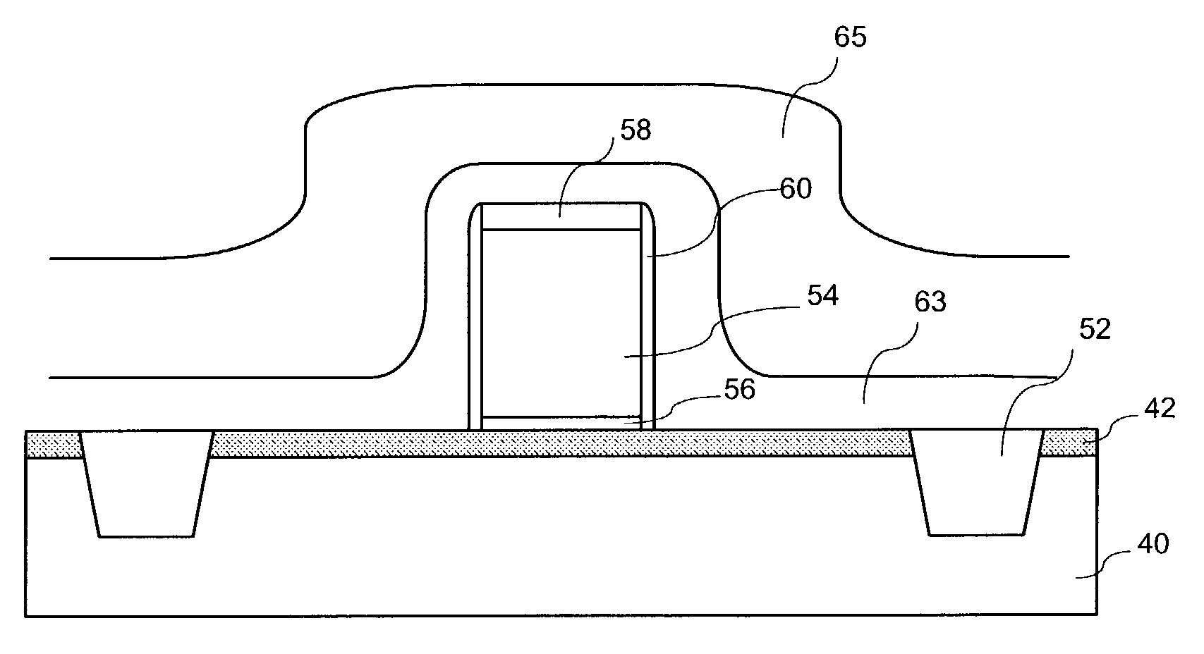
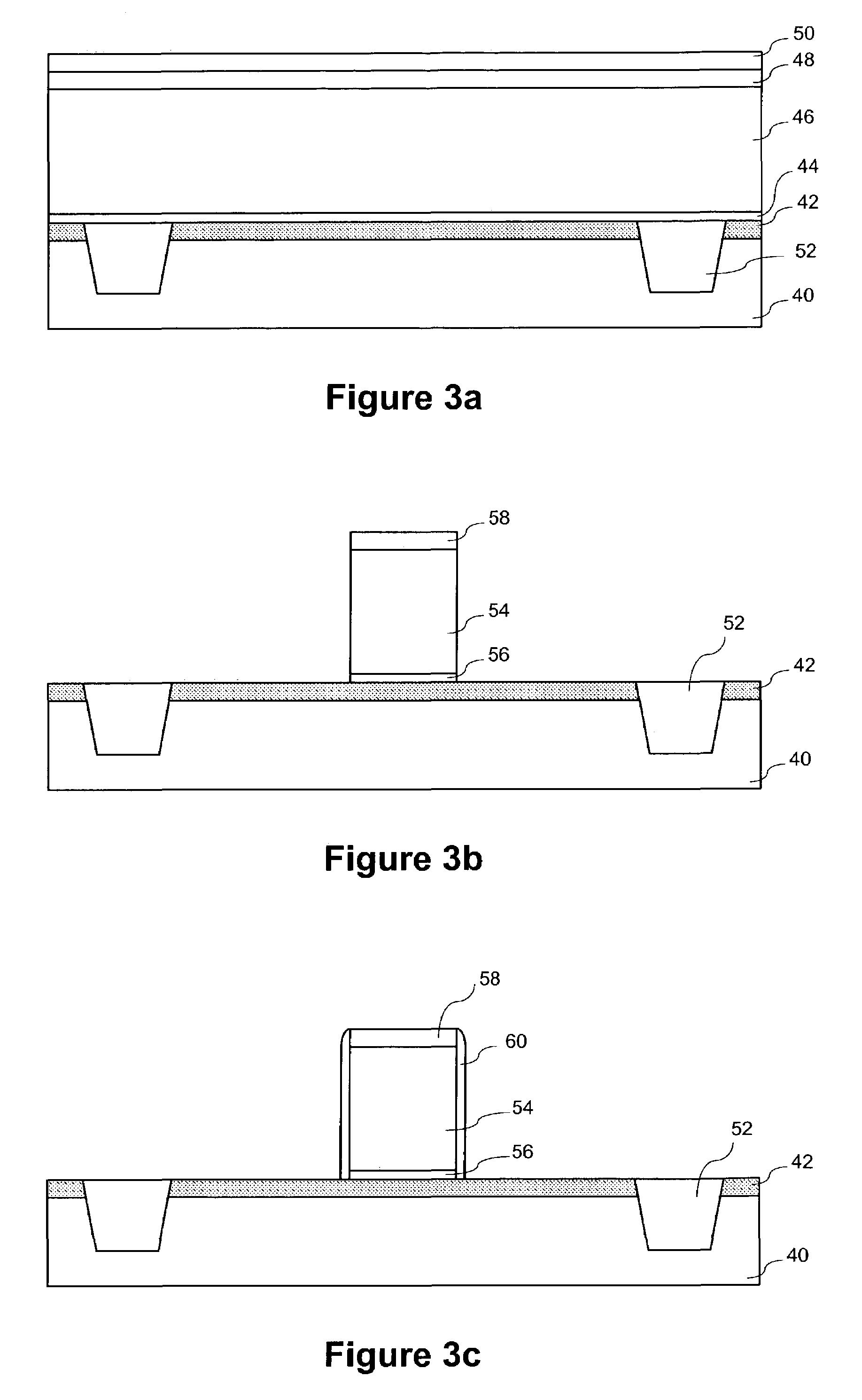
[0024]FIGS. 3a–3i illustrate structures formed during fabrication of a strained silicon MOSFET in accordance with an exemplary embodiment. FIG. 3a shows a structure comprising a layer of silicon germanium 40 having an epitaxial layer of silicon 42 formed on its surface. The silicon germanium layer 40 preferably has a composition Si1-xGex, where x is approximately 0.2, and is more generally in the range of 0.1 to 0.3.

[0025]The silicon germanium layer 40 is typically grown on a silicon wafer. Silicon germanium may be grown, for example, by chemical vapor deposition using Si2H6 (disilane) and GeH4 (germane) as source gases, with a substrate temperature of 600 to 900 degrees C., a Si2H6 partial pressure of 30 mPa, and a GeH4 partial pressure of 60 mPa. SiH4 (silane) may be used in alternative processes. Growth of the silicon germanium material may be initiated using these ratios, or alternatively the partial pressure of GeH4 may be gradually increased beginning from a lower pressure or ...


PUM


Abstract

An exemplary embodiment relates to a method for forming a metal oxide semiconductor field effect transistor (MOSFET). The method includes providing a substrate having a gate formed above the substrate and performing at least one of the following depositing steps: depositing a spacer layer and forming a spacer around a gate and gate insulator located above a layer of silicon above the substrate; depositing an etch stop layer above the spacer, the gate, and the layer of silicon; and depositing a dielectric layer above the etch stop layer. At least one of the depositing a spacer layer, depositing an etch stop layer, and depositing a dielectric layer comprises high compression deposition which increases in tensile strain in the layer of silicon.

Description

FIELD OF THE INVENTION[0001]The present disclosure relates generally to integrated circuits and methods of manufacturing integrated circuits. More particularly, the present disclosure relates to a semiconductor having a tensile strained substrate and a method of making such a semiconductor.BACKGROUND OF THE INVENTION[0002]Semiconductor manufactures utilize a wide variety of techniques to improve the performance of semiconductor devices, such as metal oxide semiconductor field effect transistors (MOSFETs). FIG. 1 shows a conventional MOSFET device. The MOSFET of FIG. 1 is fabricated on a semiconductor substrate 10 within an active area bounded by shallow trench isolations 12 that electrically isolate the active area of the MOSFET from other IC components fabricated on the substrate 10.[0003]The MOSFET is comprised of a gate electrode 14 that is separated from a channel region in the substrate 10 by a thin first gate insulator 16 such as silicon oxide or oxide-nitride-oxide (ONO). To ...

Claims


Application Information

Patent Timeline
IPC IPC(8): H01L21/4763H01L29/10
CPCH01L29/1054H01L29/7843Y10S257/90Y10S438/933H01L2924/0002H01L2924/00H01L21/18
Inventor NGO, MINH V.BESSER, PAUL R.LIN, MING RENWANG, HAIHONG
Owner ADVANCED MICRO DEVICES INC
Why Eureka
Try Eureka