
Semiconductor integrated circuit device

a technology of integrated circuits and semiconductors, applied in semiconductor devices, semiconductor/solid-state device details, electrical devices, etc., can solve problems such as fear of serious device threat, leakage of confidential information in devices, and change of device operation, so as to prevent circuit alteration and facilitate design layout

Inactive Publication Date: 2006-02-14
PANASONIC SEMICON SOLUTIONS CO LTD
View PDF8 Cites 6 Cited by
  • Summary
  • Abstract
  • Description
  • Claims
  • Application Information

AI Technical Summary

Benefits of technology

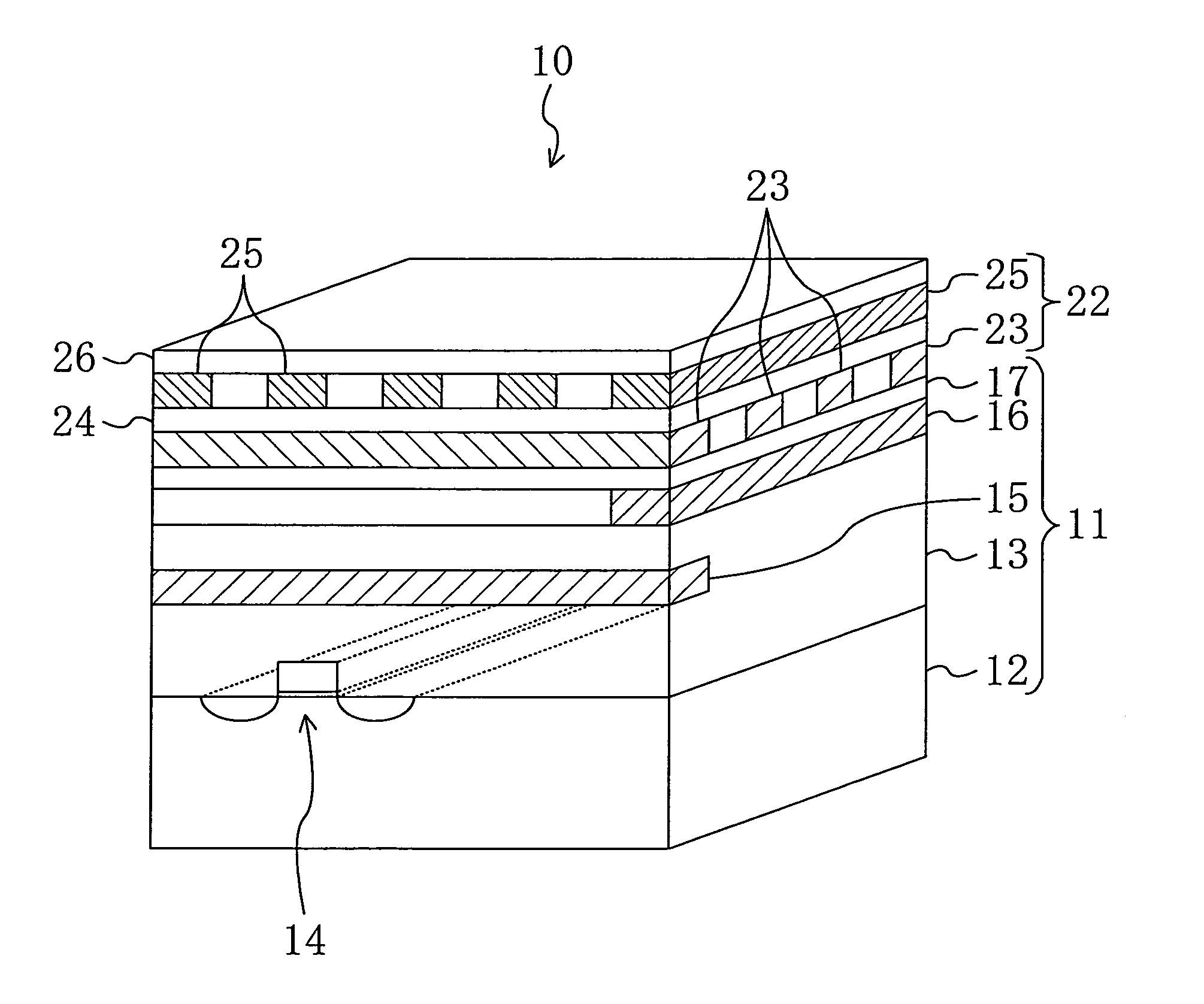
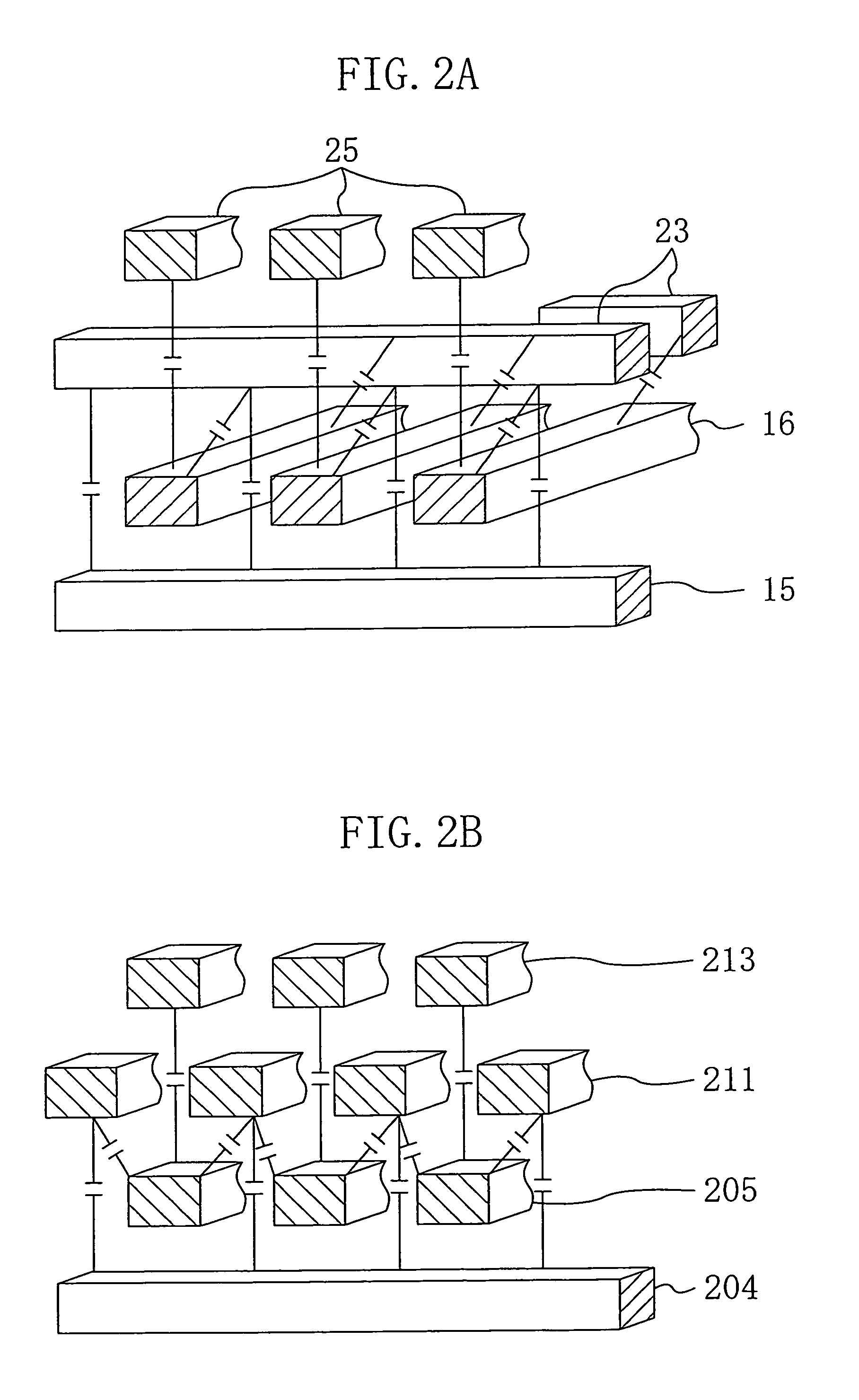
The present invention provides a semiconductor integrated circuit device with easy-to-design layout and high-security shield lines for preventing circuit alteration. The shield wiring layer includes a lower shield line and an upper shield line that intersect with each other, which averages parasitic capacitances in interconnection lines of the integrated circuit. The directions in which the shield line and an interconnection line of the integrated circuit are arranged diagonally intersect each other, making it difficult to determine the actual connections in the shield wiring layer. The device also includes a selector circuit that can change the line targeted for connection, further increasing security. The shield line can have a connector connected to a power source line, ground line, or signal line for controlling the integrated circuit, and the connector can have a plurality of connectors with random intervals or randomly arranged dummy vias to further improve security.

Problems solved by technology

In semiconductor integrated circuit devices (LSIs) requiring high levels of security, there is a fear that physical alterations might be made to circuits thereof and thereby provide change in operations of the devices, leakage of confidential information in the devices, or other disadvantages.
This fear poses a serious threat to the devices.
With this construction, it is impossible to alter the circuits without removing the upper- and lower-layer shield lines 213 and 211, which makes it more difficult to accomplish alteration.
Thus, the differently arranged (laid) directions of the LSI interconnection lines 204 and 205 create imbalances in signal delay time, which causes a problem that LSI layout design becomes extremely difficult.
Moreover, such a construction causes another problem that alteration to interconnection lines using an FIB apparatus is facilitated.

Method used


Image

  • Semiconductor integrated circuit device
  • Semiconductor integrated circuit device
  • Semiconductor integrated circuit device

Examples


first embodiment

[0042]A first embodiment of the present invention will be described with reference to the accompanying drawings.

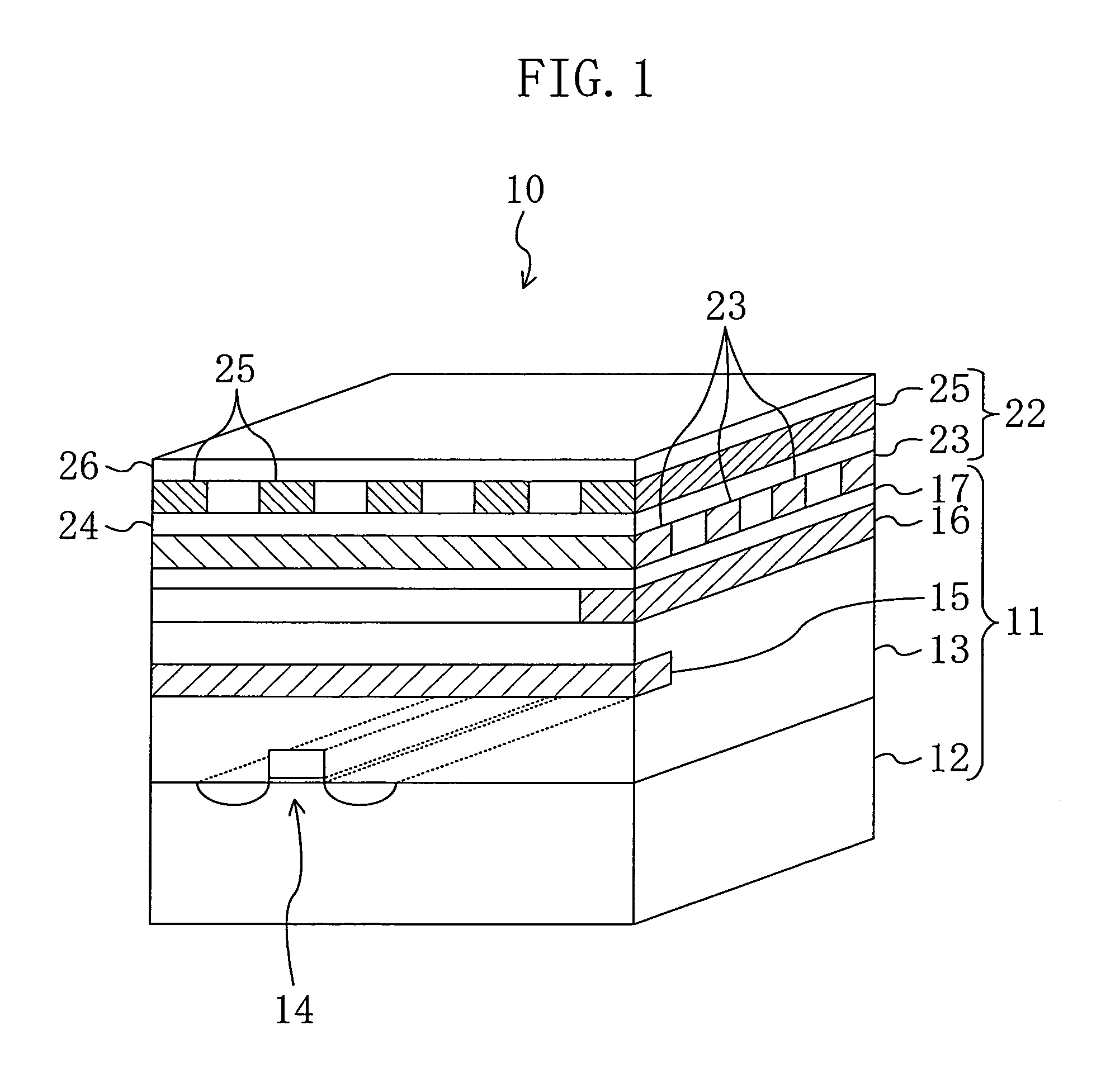
[0043]FIG. 1 schematically shows the cross-sectional structure of a semiconductor integrated circuit device provided with shield lines according to the first embodiment of the present invention.

[0044]Referring to FIG. 1, a semiconductor integrated circuit device 10 according to the first embodiment is composed of an LSI function unit 11 and a shield wiring layer 22 formed on the LSI function unit 11.

[0045]The LSI function unit 11 is formed of a semiconductor substrate 12 and a first insulating film 13, and the semiconductor substrate 12 is formed with a plurality of circuit elements including, for example, a MOS transistor 14. The first insulating film 13 is formed with first LSI interconnection lines 15 and second LSI interconnection lines 16. A second insulating film 17 is formed over the first insulating film 13.

[0046]The shield wiring layer 22 is composed of lower shie...

second embodiment

[0062]A second embodiment of the present invention will be described below with reference to the accompanying drawings.

[0063]FIGS. 5(a) and 5(b) show a semiconductor integrated circuit device according to the second embodiment of the present invention. FIG. 5(a) is a view showing the plan configuration of shield lines, and FIG. 5(b) is a partly enlarged view showing the plan arrangement of shield lines and LSI interconnection lines. Description of the components shown in FIGS. 5(a) and 5(b) that are the same as those shown in FIG. 1 will be omitted by retaining the same reference numerals.

[0064]Referring to FIG. 5(a), shield lines 52 in the second embodiment are spaced in a folded arrangement to extend in parallel with one diagonal line of the semiconductor integrated circuit device (chip) 10 in square plan shape. In this embodiment, each of the shield lines 52 may be composed of a single layer or double layers. If each of the shield lines 52 is composed of double layers, such as up...

third embodiment

(Modification of Third Embodiment)

[0083]A modification of the third embodiment of the present invention will be described below with reference to FIG. 9.

[0084]Referring to FIG. 9, a plurality of selector circuits 61 are arranged not only at the ends of the shield lines 60 but also at positions on the integrated circuit (not shown) so that the selector circuits 61 are spaced at random intervals.

[0085]Each of the selector circuits 61 switches target terminals to be connected to the respective shield lines in a similar manner to the third embodiment. The schematic line denoted by the reference numeral 67 is a line composed of electrically connected shield lines of the multiple shield lines 60.

[0086]With this configuration, the connections between the shield lines 60 can be changed more complicatedly. This provides a more greatly improved level of security to the device.

[0087]Note that in the third embodiment and its modification, the shield lines 60 preferably have the configuration sh...


PUM


Abstract

A semiconductor integrated circuit device (10) is composed of an LSI function unit (11) and a shield wiring layer (22) formed on the unit. The LSI function unit (11) includes a semiconductor substrate (12) and a first insulating film (13), and the semiconductor substrate (12) is formed with a circuit element including, for example, a MOS transistor (14). The shield wiring layer (22) is composed of a lower shield line (23), a third insulating film (24), an upper shield line (25), and a fourth insulating film (26) sequentially stacked above a second insulating film (17). The directions in which the lower and upper shield lines (23) and (25) are arranged intersect each other.

Description

TECHINICAL FIELD[0001]The present invention relates to semiconductor integrated circuit devices, such as IC cards, of which high levels of security are demanded and which have means for preventing physical alterations.BACKGROUND ART[0002]In semiconductor integrated circuit devices (LSIs) requiring high levels of security, there is a fear that physical alterations might be made to circuits thereof and thereby provide change in operations of the devices, leakage of confidential information in the devices, or other disadvantages. This fear poses a serious threat to the devices.[0003]The alterations mentioned above are generally made in such a manner that using a focused ion beam (FIB) apparatus, an upper portion of an LSI is radiated with ion beams to cut interconnection lines of the LSI and to deposit metal for use in interconnection, and that a piece of the cut interconnection line is electrically connected to another interconnection line located around the cut interconnection line.[...

Claims


Application Information

Patent Timeline
Patent Type & Authority Patents(United States)
IPC IPC(8): H01L27/10H01L23/522H01L23/528H01L23/58
CPCH01L23/5222H01L23/5225H01L23/528H01L23/576H01L2924/0002Y10S257/922H01L2924/00
Inventor ITOH, RIEMATSUNO, NORIAKITSUNODA, MASATO
Owner PANASONIC SEMICON SOLUTIONS CO LTD
Learn More