Eureka AIR delivers breakthrough ideas for toughest innovation challenges, trusted by R&D personnel around the world.

Electroless nickel immersion gold semiconductor flip chip package

a technology of flip chip and nickel immersion, which is applied in the direction of electrical apparatus construction details, manufacturing tools, and soldering apparatus, etc., can solve the problems of achieve greater package reliability and fewer fractured solder bonds

Inactive Publication Date: 2006-01-31
ALTERA CORP
View PDF5 Cites 6 Cited by
  • Summary
  • Abstract
  • Description
  • Claims
  • Application Information

AI Technical Summary

Benefits of technology

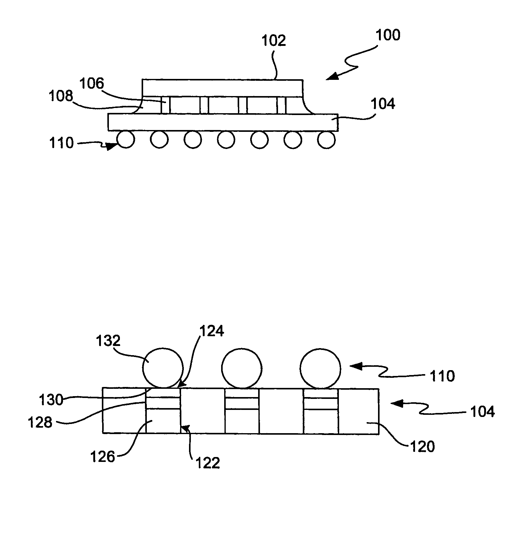
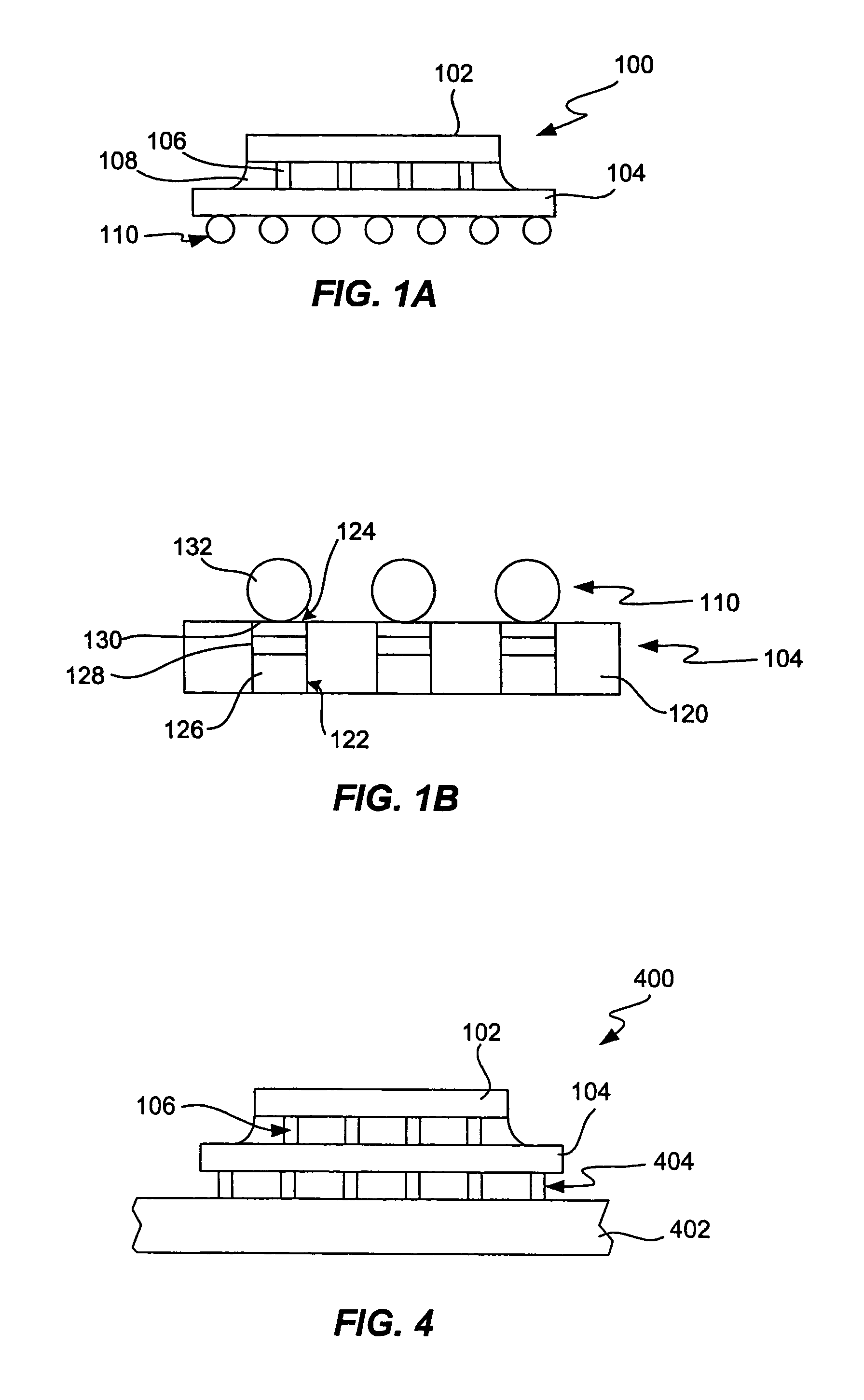
[0010]To achieve the foregoing, the present invention provides a flip chip package, apparatus and technique in which a ball grid array composed of a doped eutectic Pb / Sn solder composition is used. The dopant in the Pb / Sn solder forms a compound or complex with the phosphorous residue from the electroless nickel plating process that is mixable with the Pb / Sn solder. The phosphorous containing compound or complex. The phosphorous containing compound or complex prevents degradation of the solder / under bump metallization bond associated with phosphorus residue. The interfacial solder / under bump metallization bond is thereby strengthened. This results in fewer fractured solder bonds and greater package reliability. The amount of the metal dopant is generally greater than 0.2% by weight, for example about 0.2% to 2.5%, or about 2%. Sample dopants include Al, Fe, Ni, Cu, Zn, Mo and In. An electronic device composed of a package in accordance with the invention mounted on a printed circuit board, and a method of making such an electronic device are also provided.

Problems solved by technology

This results in fewer fractured solder bonds and greater package reliability.

Method used


Image

  • Electroless nickel immersion gold semiconductor flip chip package
  • Electroless nickel immersion gold semiconductor flip chip package
  • Electroless nickel immersion gold semiconductor flip chip package

Examples


example 1

Cu-Doped Solder Balls

[0030]

Production Lot No.PA21210-Cu762Solder Ball Quantity250kAlloy CompositionSn62Pb36Cu2Solder Ball Size0.762 ± 0.0254 (mm)

Chemical Composition (Atomic Absorption)

[0031]

ElementActual CompositionSn61.940PbBalanceCu 2.1200

Melting Temperature & Specific Gravity

[0032]

Actual StatusMelting Temp. (° C.)180.86Specific Gravity8.50

Dimension Inspection (Profile Projector)

[0033]

Avg. Solder Ball Size (mm)0.7619Standard Deviation0.0042Max. Solder Ball Size (mm)0.776Min. Solder Ball Size (mm)0.751Cp2.0069Cpk1.9997Out of Spec. Criteria (ea)0 / 1,000

Visual Inspection (SEM. Stereomicroscope)[0034]No Cracks, no scratches, and no protrusions

example 2

Zn-Doped Solder Balls

[0035]

Production Lot No.PA21210-Zn762Solder Ball Quantity250kAlloy CompositionSn62Pb36Zn2Solder Ball Size0.762 ± 0.0254 (mm)

Chemical Composition (Atomic Absorption)

[0036]

ElementActual CompositionSn62.350PbBalanceZn 2.4000

Melting Temperature and Specific Gravity

[0037]

Actual StatusMelting Temp. (° C.)172.46Specific Gravity7.60

Dimension Inspection (Profile Projector)

[0038]

Avg. Solder Ball Size (mm)0.7617Standard Deviation0.0045Max. Solder Ball Size (mm)0.774Min. Solder Ball Size (mm)0.750Cp1.8994Cpk1.8786Out of Spec. Criteria (ea)0 / 1,000

Visual Inspection (SEM Stereomicroscope)[0039]No Cracks, no scratches, and no protrusions

example 3

In-Doped Solder Balls

[0040]

Production Lot No.PA21210-In762Solder Ball Quantity250kAlloy CompositionSn62Pb36In2Solder Ball Size0.762 ± 0.0254 (mm)

Chemical Composition (Atomic Absorption)

[0041]

ElementActual CompositionSn63.760PbBalanceIn 2.0300

Melting Temperature and Specific Gravity

[0042]

Actual StatusMelting Temp. (° C.)172.25Specific Gravity7.60

Dimension Inspection (Profile Projector)

[0043]

Avg. Solder Ball Size (mm)0.7614Standard Deviation0.0042Max. Solder Ball Size (mm)0.774Min. Solder Ball Size (mm)0.749Cp2.0220Cpk1.9722Out of Spec. Criteria (ea)0 / 1,000

Visual Inspection (SEM Stereomicroscope)[0044]No Cracks, no scratches, and no protrusions


PUM

PropertyMeasurementUnit
Fractionaaaaaaaaaa
Percent by massaaaaaaaaaa

Abstract

A flip chip package, apparatus and technique in which a ball grid array composed of a doped eutectic Pb / Sn solder composition is used. The dopant in the Pb / Sn solder forms a compound or complex with the phosphorous residue from the electroless nickel plating process that is mixable with the Pb / Sn solder. The phosphorous containing compound or complex prevents degradation of the solder / under bump metallization bond associated with phosphorus residue. The interfacial solder / under bump metallization bond is thereby strengthened. This results in fewer fractured solder bonds and greater package reliability.

Description

CROSS-REFERENCE TO RELATED APPLICATIONS[0001]This application is a continuation of U.S. patent application Ser. No. 10 / 382,784 filed Mar. 5, 2003, titled INTERFACIAL STRENGTHENING FOR ELECTROLESS NICKEL IMMERSION GOLD SUBSTRATES (now U.S. Pat. No. 6,756,687, issued Jun. 29, 2004), which is incorporated herein by reference in its entirely and for all purposes.BACKGROUND OF THE INVENTION[0002]1. Field of the Invention[0003]This invention relates generally to integrated circuit packaging, and in particular to flip chip packaging. More specifically, the invention relates to compositions and techniques for strengthening the interfacial bond between a flip chips package substrate and the solder balls used for external electrical connection of the completed flip chip package.[0004]2. Description of Related Art[0005]In integrated circuit packaging, a semiconductor die (also referred to as an integrated circuit (IC) or “chip”) may be bonded directly to a packaging substrate, without the need...

Claims


Application Information

Patent Timeline
IPC IPC(8): H01L23/48H01L21/56H01L23/31H01L23/498H05K3/24H05K3/34
CPCH01L21/563H01L23/49816H05K3/3463H01L23/3128Y10T29/49126H01L2224/73203H01L2924/01078H01L2924/01079H05K3/244H05K2201/10734H01L2924/01322H01L2224/16225H01L2224/32225H01L2224/73204H01L2924/00H01L2924/00014H01L2224/0401
Inventor NGUYEN, MY
Owner ALTERA CORP
Why Eureka
Eureka Blog
Learn More