Method of manufacturing semiconductor device

Inactive Publication Date: 2005-12-27
SK HYNIX INC
View PDF4 Cites 1 Cited by
  • Summary
  • Abstract
  • Description
  • Claims
  • Application Information

AI Technical Summary

Benefits of technology

[0016]Accordingly, the present invention has been made to solve the above-mentioned problems occurring in the prior art, and an object of the present invention is to provide a method of manufacturing a semiconductor device, which prevents contact resistance due to a native oxide film from being increased.
[0020]According to the present invention, after the contact hole is washed, sputtering or chemical vapor deposition equipment provides a reducing gas such as a hydrogen gas to a contact surface to remove a native oxide film formed on the contact surface. Furthermore, the impurity concentration on a surface of the junction region is increased by additional in-situ doping step. The equipment deposits a contact conductive film into the contact surface in-situ, so that a clean contact surface from which the native oxide film is removed is provided. Accordingly, a contact resistance due to the native oxide film from being efficiently prevented.

Problems solved by technology

In the contact process techniques, when a contact between upper and lower patterns is unstable or a contact resistance increases, although a fine adjustment of a pattern is achieved, the reliability of the semiconductor device is lacking and it is difficult to perform a high speed operation thereof.
However, during the formation of a contact conductive film, since the deposition of a metal film in sputtering equipment or the deposition of a polycrystalline silicon film in chemical vapor deposition equipment is achieved after the washed substrate surface is exposed to air, as shown in FIG. 3, the formation of a native oxide film 10 at a contact surface is unavoidable.
This causes the semiconductor device to be degraded.
However, such steps minimize the influence of the native oxide film and do not provide a clean contact surface, causing the increase of the contact resistance according to badness of the contact surface.

Method used


Image

  • Method of manufacturing semiconductor device
  • Method of manufacturing semiconductor device
  • Method of manufacturing semiconductor device

Examples


Embodiment Construction

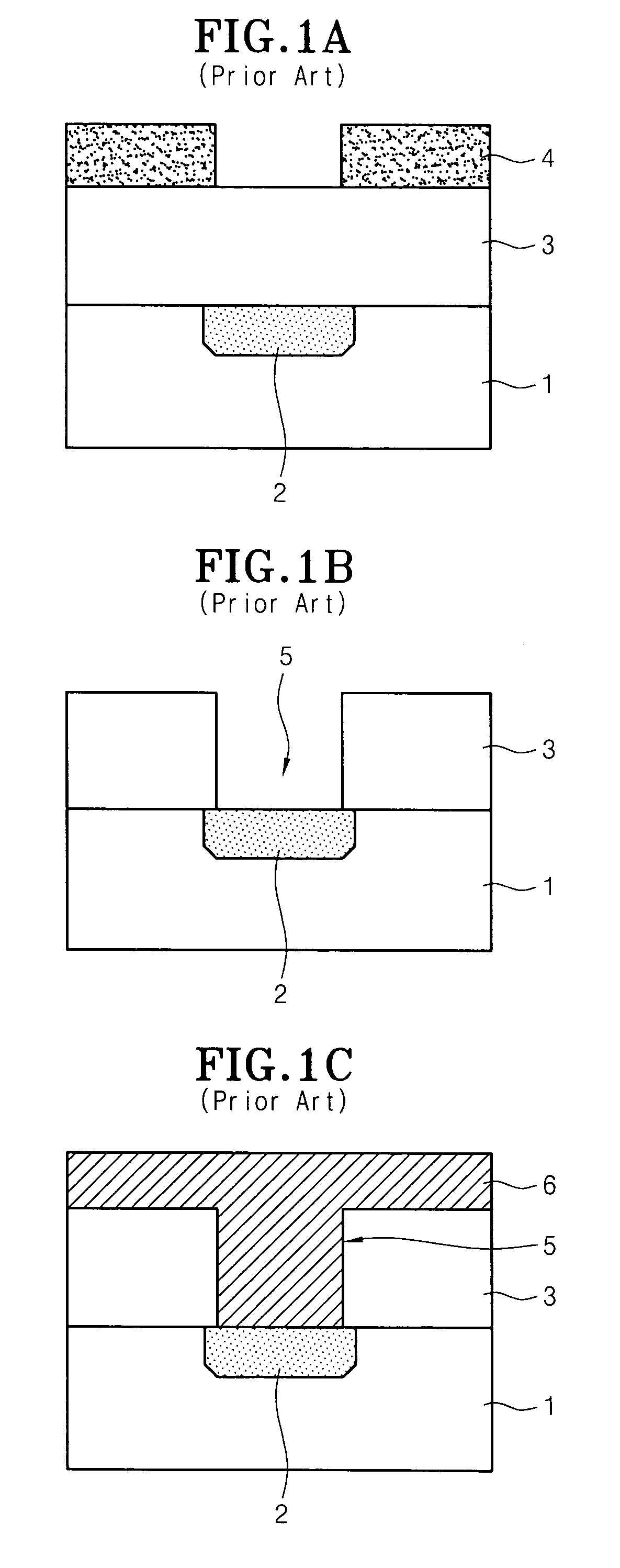
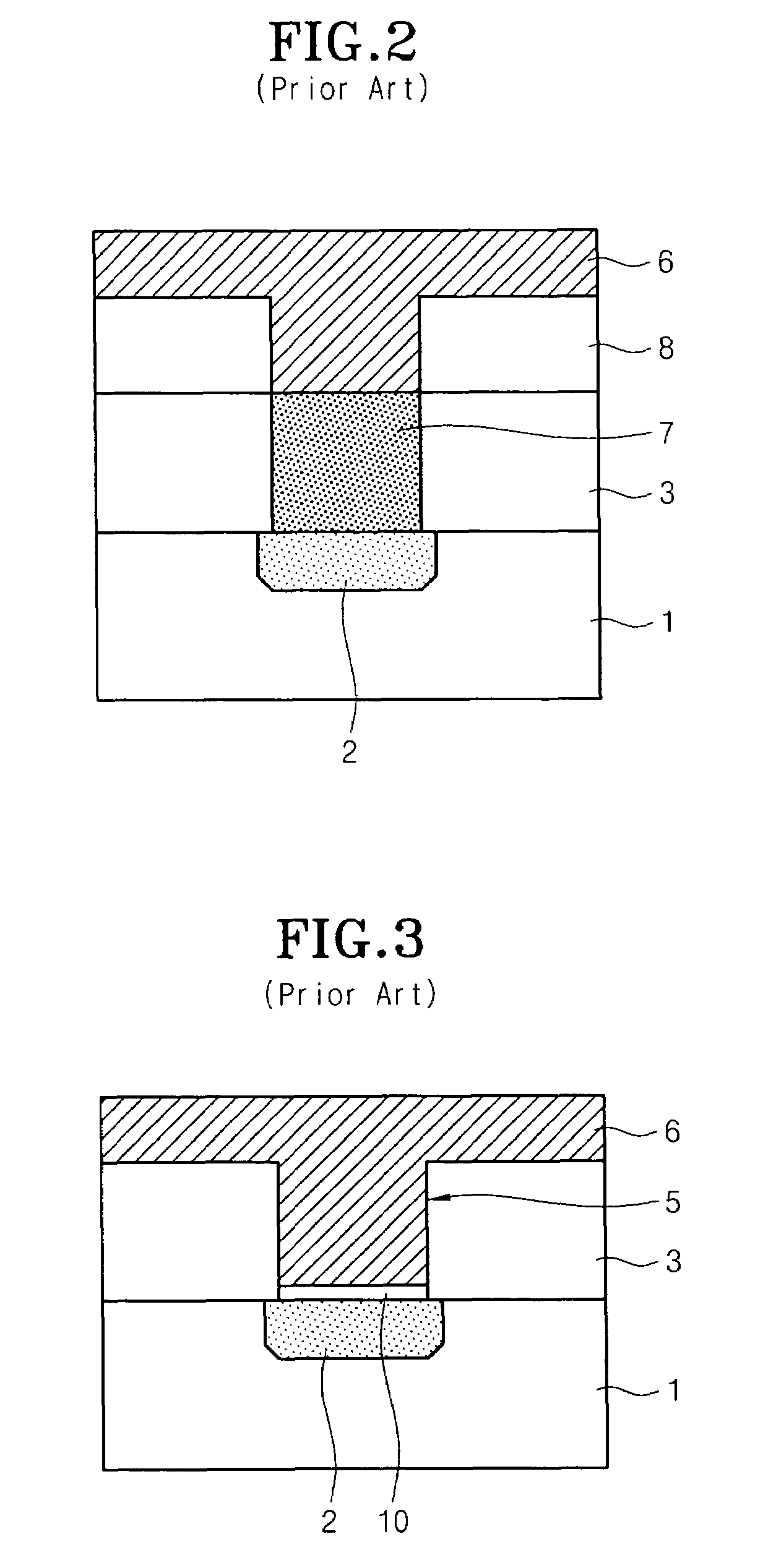
[0026]Hereinafter, a preferred embodiment of the present invention will be described with reference to the accompanying drawings. In the following description and drawings, the same reference numerals are used to designate the same or similar components, and so repetition of the description on the same or similar components will be omitted.

[0027]FIGS. 4A through 4D are cross-sectional views which illustrate a method of manufacturing a semiconductor device according to an embodiment of the present invention.

[0028]Referring to FIG. 4A, a silicon substrate 41 on which a predetermined lower structure having a junction region 42 is formed is prepared. In the junction region 42, a conductivity of a semiconductor is adjusted according to a kind of an impurity, an impurity concentration, and an impurity depth.

[0029]Referring to FIG. 4B, an interlayer dielectric film 43 is deposited over a whole surface of the silicon substrate 41 to cover the lower structure having the junction region 42. T...


PUM


Abstract

Disclosed is a method of manufacturing a semiconductor device, which prevents a contact resistance due to a native oxide film from being increased. Semiconductor substrate on which a lower structure having a junction region is formed is prepared. Interlayer dielectric film is formed over a whole surface of semiconductor substrate. Contact hole exposing the junction region is formed by etching interlayer dielectric film. Dry-cleaning and wet-cleaning for a substrate surface exposed by the contact hole are sequentially performed. Washed contact surface is preliminarily treated under reducing gas atmosphere to remove a native oxide film formed on contact surface. Impurity is additionally doped to a surface of the junction region in-situ so that impurity damages on preliminary-treated contact surface are compensated for. Conductive film is deposited on the contact hole and the interlayer dielectric film in-situ.

Description

BACKGROUND OF THE INVENTION[0001]1. Field of the Invention[0002]The present invention relates to a method of manufacturing a semiconductor device, and more particularly to a method of manufacturing a semiconductor device which prevents contact resistance due to a native oxide film from being increased.[0003]2. Description of the Prior Art[0004]As generally known in the art, in addition to the advancement of semiconductor techniques, development of high speed operation and high integration of semiconductor devices are in progress. Accordingly, fine adjustment and high integration of a pattern have been necessary. In accordance with such a tendency, various process techniques have been developed and used to obtain excellent device characteristics.[0005]In particular, in order to improve the operation performance of semiconductor devices, new contact process techniques have been developed. In the contact process techniques, when a contact between upper and lower patterns is unstable or...

Claims


Application Information

Patent Timeline
IPC IPC(8): H01L21/28H01L21/02H01L21/223H01L21/285H01L21/306H01L21/311H01L21/324H01L21/768
CPCH01L21/02063H01L21/2236H01L21/28512H01L21/76828H01L21/76814H01L21/76826H01L21/324H01L21/28
Inventor LEE, SEOK KIUKIM, IL WOOK
Owner SK HYNIX INC
Why Eureka
Try Eureka