Clock multiplier

Active Publication Date: 2005-12-20
INTEGRATED SILICON SOLUTION
View PDF5 Cites 70 Cited by
  • Summary
  • Abstract
  • Description
  • Claims
  • Application Information

AI Technical Summary

Benefits of technology

[0008]The objective of the present invention is to provide a clock multiplier capable of steadily controlling the output clock, so as to overcome the sensitivity of process drifting or temperature variation. Ideally, the clock multiplier can control the duty cycle of the output clock to be 50% to ascertain the output clock as having good quality.
[0009]The clock multiplier of the present invention comprises a first clock multiplication circuit, an inverter, a first low pass filter (LPF), a second LPF and an amplifier, the first clock multiplication circuit being operative to multiply the frequency of an input clock, the inverter being operative to invert the input clock, the first LPF receiving the output clock of the inverter for being charged or discharged, the second LPF receiving the output clock of the first clock multiplication circuit for being charged or discharged, and the amplifier being operative to compare the output voltages of the first LPF and the second LPF to perform a feedback control, so as to modulate the duty cycle of the output clock of the first multiplication clock to approach 50%. If the input clock has a full voltage swing, a one-half supply voltage (VDD / 2) can be selected as a reference voltage to substitute the inverter and the first LPF for simplifying the circuitry.

Problems solved by technology

Because of the high circuit complexity, the cost of silicon processing and testing overhead typically preclude the use of such PLLs in cost-sensitive integrated circuits.
Although the clock doubler is much simpler and cheaper, it still suffers from two limitations.
First, the useful frequency range is limited as a fixed delay line is used.
Secondly, the delay line is a circuit constituted by resistor-capacitor (RC) components, which are easily affected by process, temperature, supply voltage and clock frequency change, so the duty cycle of the delay line will be changed.
However, current clock multipliers are either more costly or ineligible, and thus it is necessary to develop a low-cost clock multiplier capable of adjusting the duty cycle of the output clock.

Method used


Image

  • Clock multiplier
  • Clock multiplier
  • Clock multiplier

Examples


first embodiment

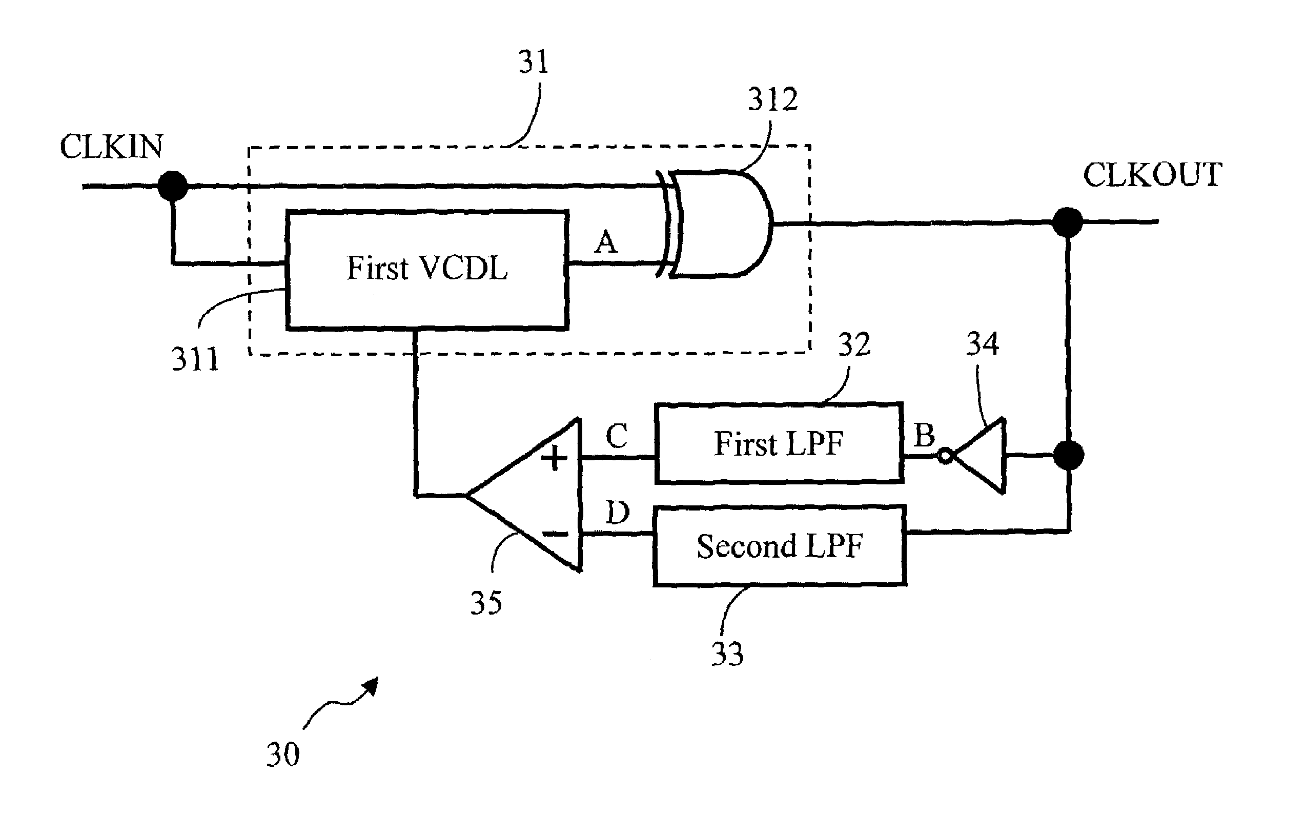
[0023]FIG. 3 illustrates the circuitry of a 2X clock multiplier 30 of the present invention, and the corresponding timings of the points in FIG. 3 are shown in FIG. 4. The 2X clock multiplier 30 comprises a first clock multiplication circuit 31, an inverter 34, a first LPF 32, a second LPF 33 and an operational amplifier 35, the first clock multiplication circuit 31 receiving a CLKIN, and outputting a CLKOUT. The CLKOUT can be controlled by the feedback loop of the inverter 34, the first LPF 32, the second LPF 33 and the operational amplifier 35. The first clock multiplication circuit 31 consists of a first VCDL 311 and a first XOR gate 312. The CLKIN is as one input to the first OR gate 312, and a delayed T / 4 clock generated from the first VCDL 311 is as the other one. Accordingly, the frequency of the CLKOUT outputted from the first XOR gate 312 doubles that of the CLKIN.

[0024]Theoretically, if the first VCDL 311 can exactly delay the CLKIN by T / 4, the duty cycle of the CLKOUT wil...

second embodiment

[0025]If the CLKIN has a full voltage swing, the high voltage is equivalent to the supply voltage VDD, and the low voltage is equivalent to ground. Therefore, a reference voltage VDD / 2 can be selected to substitute the inverter 34 and the first LPF 32 to form a 2X clock multiplier 50, the present invention, shown as in FIG. 5. Likewise, such manner can also apply to the following embodiments as an alternative.

[0026]FIG. 6 illustrates the circuitry of a 3X clock multiplier 60 using the above-mentioned manner, and FIG. 7 shows the corresponding timings of the points shown in FIG. 6. The 3X clock multiplier 60 comprises a first clock multiplication circuit 61, an inverter 64, a first LPF 62, a second LPF 63 and an operational amplifier 65. The first clock multiplication circuit 61 receives a CLKIN and outputs a CLKOUT, which may be controlled by the feedback loop of the inverter 64, the first LPF 62, the second LPF 63 and the operational amplifier 65 so as to modulate the clock delay o...

fourth embodiment

[0027]FIG. 8 illustrates the circuitry of a 4X clock multiplier 80 of the present invention, and FIG. 9 shows the corresponding timings of the points shown in FIG. 8. The 4X clock multiplier 80 is associated with two 2X clock multipliers, iteratively doubling the frequency of a CLKIN from 2X to 4X. The 4X clock multiplier 80 comprises a first clock multiplication circuit 81, a second clock multiplication circuit 86, an inverter 84, a first LPF 82, a second LPF 83 and an operational amplifier 85, the first clock multiplication circuit 86 including a first VCDL 814 and a first XOR gate 813, functioning as the first VCDL 31 of the 2X clock multiplier 30 for doubling the frequency of the CLKIN, and the second clock multiplication circuit 86 including a second VCDL 861 and a second XOR gate 862. The CLKIN and the output of the first VCDL 814, i.e., the clock “A,” are inputted to the first XOR gate 813, and the output clock of the first XOR gate 813, designated as CLK2X, has double the fr...


PUM


Abstract

A clock multiplier capable of modulating the duty cycle of the output clock comprises a first clock multiplication circuit, an inverter, a first low pass filter, a second low pass filter and an amplifier, the first multiplication clock being operative to multiply the frequency of an input clock, the inverter being operative to invert the input clock, the first low pass filter receiving the output clock of the inverter for being charged or discharged, the second low pass filter receiving the output clock of the first clock multiplication circuit for being charged or discharged, the amplifier being operative to compare the output voltages of the first low pass filter and the second low pass filter to perform a feedback control, so as to modulate the duty cycle of the output clock of the first multiplication clock to approach 50%.

Description

BACKGROUND OF THE INVENTION[0001](A) Field of the Invention[0002]The present invention is related to a clock multiplier, more specifically, to a clock multiplier capable of modulating the duty cycle of the output clock.[0003](B) Description of Related Art[0004]With the rising demand of higher clock frequency to semiconductor devices, on-chip clock multipliers are widely used nowadays. Conventionally, the relatively expensive phase-lock loops (PLLs) and lower-cost clock doublers are chosen as multiplication solutions.[0005]FIG. 1 illustrates a function block diagram of a clock multiplier 10 using PLL technique, which consists of a divided-by-M counter 11, a phase-frequency detector 12, a charge pump 13, a loop filter 14, a voltage-controlled oscillator (VCO) 15 and a divided-by-N counter 16. In accordance with such design, the frequency of the output clock (CLKOUT) is equivalent to that of the input clock (CLKIN) multiplied by N / M. Because of the high circuit complexity, the cost of ...

Claims


Application Information

Patent Timeline
IPC IPC(8): H03B19/00H03K5/156
CPCH03K5/1565
Inventor CHIN-CHIEH, CHAOCHAO-PING, SUYEN-KUANG, CHEN
Owner INTEGRATED SILICON SOLUTION
Why Eureka
Try Eureka