
Floating-gate semiconductor structures

a technology of semiconductor structure and floating gate, which is applied in the direction of semiconductor devices, digital storage, instruments, etc., can solve the problems of low transistor breakdown voltage, large scaling challenge of silicon integrated circuit processing to deep submicron feature size, and poor transistor matching

Inactive Publication Date: 2005-11-15
SYNOPSYS INC +1
View PDF73 Cites 50 Cited by
  • Summary
  • Abstract
  • Description
  • Claims
  • Application Information

AI Technical Summary

Problems solved by technology

The scaling of silicon integrated-circuit processing to deep-submicron feature sizes poses significant challenges for SOC (systems-on-a-chip) design.
On the negative side, scaling burdens analog CMOS with low transistor-breakdown voltages, poor transistor matching, and limited dynamic range.
Unfortunately, large-scale local learning in silicon has so far eluded researchers.
A primary reason is the lack of a simple way to enable nonvolatile analog on-line adaptation in CMOS circuits.
Although the advantages of using floating gate transistors as memory elements are well known, their application to silicon learning networks and analog memory cells has been limited.
The principal reason has been the lack of suitable bidirectional and self-convergent mechanisms for writing the analog memory.
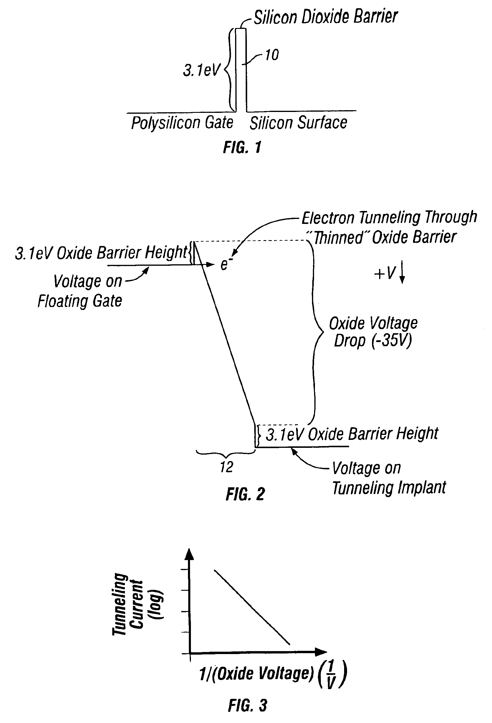
Alternatively, an electron could tunnel through this barrier; however, at the oxide thicknesses required for nonvolatile storage the tunneling probability is also exceedingly small.
Both approaches are unattractive.
The dual polarity solution requires a negative voltage much lower than the substrate potential; the single polarity solution does not support simultaneous memory reading and writing or self-convergent memory writes.
Although excess charge is acceptable when writing a binary valued “digital” memory, where the exact quantity of charge is irrelevant once it exceeds the amount necessary to completely switch the device to one of its two binary states, uncertainty in the amount of charge applied to an analog memory cell may result in significant memory error.
This need has not been satisfied adequately by commercial nFET (n-channel field effect transistor) EEPROMs, primarily because conventional EEPROM transistors do not permit simultaneous memory reading and writing.
Unfortunately, since the control gate modulates the injection rate but does not receive the injected charge, the memory cannot be both written and read simultaneously.
Such a device is acceptable for digital EEPROMs but is unsuitable for analog learning cell or analog memory applications.
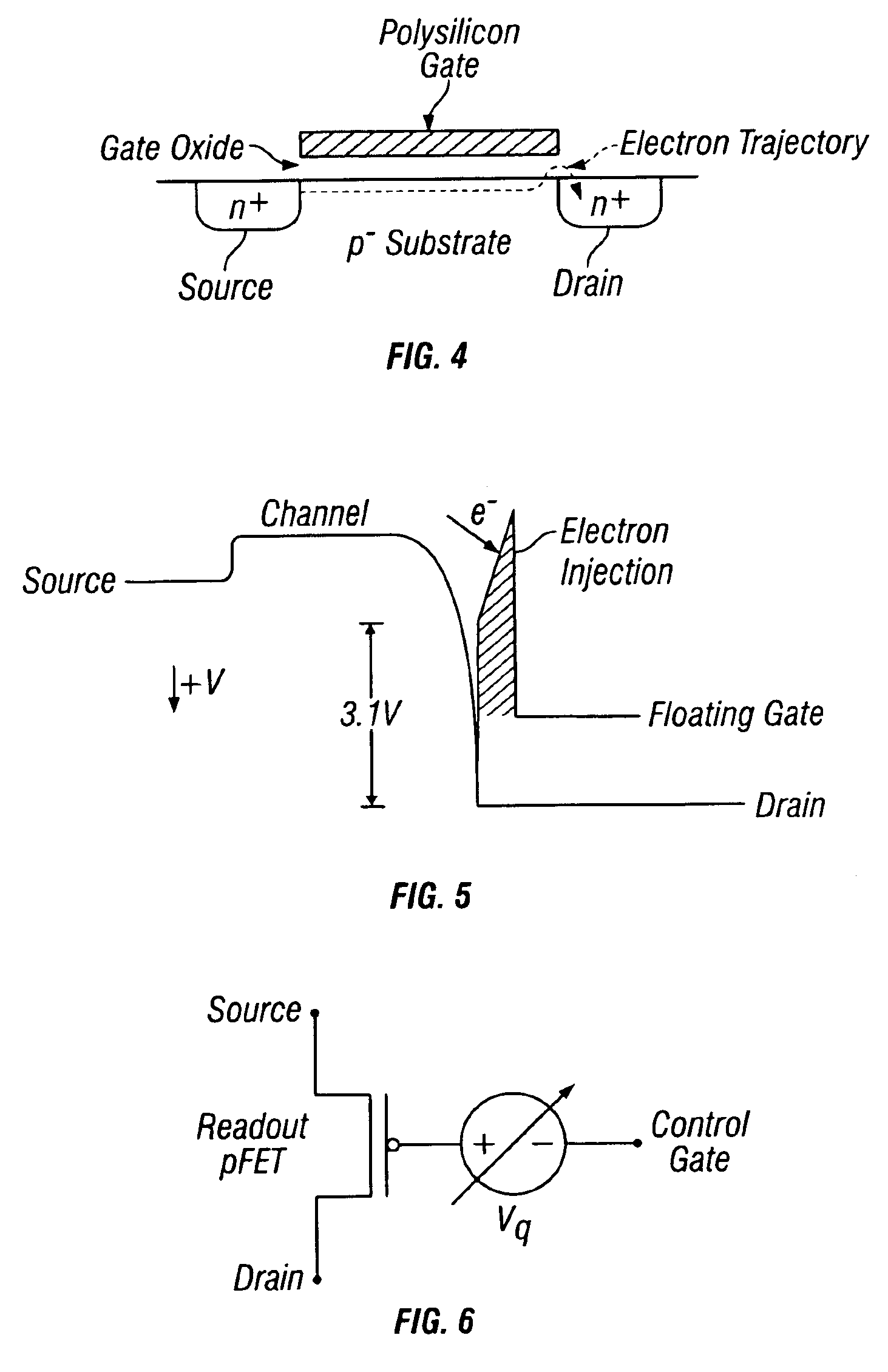
The disadvantage of this device is that in order to achieve injection, both the drain and gate voltages must exceed approximately 2.5 volts which results in high channel current and consequent high power consumption.
Additional steps, for example double-polysilicon processes, increase the cost of fabricating such memory devices.

Method used


Image

  • Floating-gate semiconductor structures
  • Floating-gate semiconductor structures
  • Floating-gate semiconductor structures

Examples


Embodiment Construction

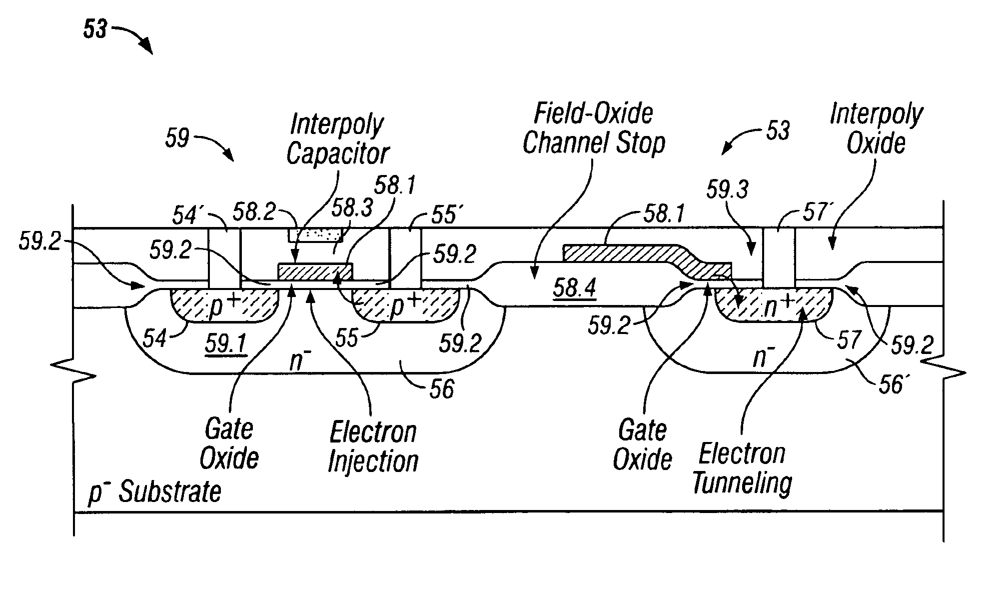
[0061]Embodiments of the present invention are described herein in the context of floating gate semiconductor structures. Those of ordinary skill in the art will realize that the following detailed description of the present invention is illustrative only and is not intended to be in any way limiting. Other embodiments of the present invention will readily suggest themselves to such skilled persons having the benefit of this disclosure. Reference will now be made in detail to implementations of the present invention as illustrated in the accompanying drawings. The same reference indicators will be used throughout the drawings and the following detailed description to refer to the same or like parts.

[0062]In the interest of clarity, not all of the routine features of the implementations described herein are shown and described. It will, of course, be appreciated that in the development of any such actual implementation, numerous implementation-specific decisions must be made in order...


PUM


Abstract

Hot-electron injection driven by hole impact ionization in the channel-to-drain junction of a p-channel MOSFET provides a new mechanism for writing a floating-gate memory. Various pFET floating-gate structures use a combination of this mechanism and electron tunneling to implement nonvolatile analog memory, nonvolatile digital memory, or on-line learning in silicon. The memory is nonvolatile because the devices use electrically isolated floating gates to store electronic charge. The devices enable on-line learning because the electron injection and tunneling mechanisms that write the memory can occur during normal device operation. The memory updates and learning are bidirectional because the injection and tunneling mechanisms add and remove electrons from the floating gate, respectively. Because the memory updates depend on both the stored memory and the pFETs terminal voltages, and because they are bidirectional, the devices can implement on-line learning functions.

Description

CROSS-REFERENCE TO RELATED APPLICATIONS[0001]This application is a continuation-in-part of U.S. patent application Ser. No. 09 / 699,059 filed Oct. 27, 2000 in the names of Christopher J. Diorio and Carver A. Mead, now U.S. Pat. No. 6,452,835 issued on Sep. 17, 2002 and commonly owned herewith. That application is, in turn, a continuation of U.S. patent application Ser. No. 09 / 201,327 filed Nov. 30, 1998, now U.S. Pat. No. 6,144,581 issued on Nov. 7, 2000. U.S. patent application Ser. No. 09 / 201,327 is a divisional of U.S. patent application Ser. No. 08 / 882,717 filed Jun. 25, 1997, now U.S. Pat. No. 5,898,613 issued on Apr. 27, 1999 which is, in turn, a continuation-in-part of: (1) U.S. patent application Ser. No. 08 / 690,198 filed Jul. 26, 1996, now U.S. Pat. No. 5,825,063 issued on Oct. 20, 1998; (2) U.S. patent application Ser. No. 08 / 721,261 filed Sep. 26, 1996, now U.S. Pat. No. 5,875,126 issued on Feb. 23, 1999; and (3) U.S. patent application Ser. No. 08 / 845,018 filed Apr. 22, 1...

Claims


Application Information

Patent Timeline
Patent Type & Authority Patents(United States)
IPC IPC(8): G11C11/54G11C11/34H01L21/8247H01L27/115H01L29/788H01L29/792
CPCH01L27/115H01L27/11521H01L29/7885H01L29/66825H01L29/7883H01L27/11558H10B69/00H10B41/30H10B41/60
Inventor DIORIO, CHRISTOPHER J.HUMES, TODD E.
Owner SYNOPSYS INC
Learn More