Semiconductor device and method of manufacturing the same
a semiconductor and semiconductor technology, applied in the field of semiconductor devices, can solve the problems of large device size, high cost, and high cost, and achieve the effects of low viscosity, high reliability of devices fabricated, and significant increase of adhesion strength
- Summary
- Abstract
- Description
- Claims
- Application Information
AI Technical Summary
Benefits of technology
Problems solved by technology
Method used
Image
Examples
first embodiment
[0104](First Embodiment)
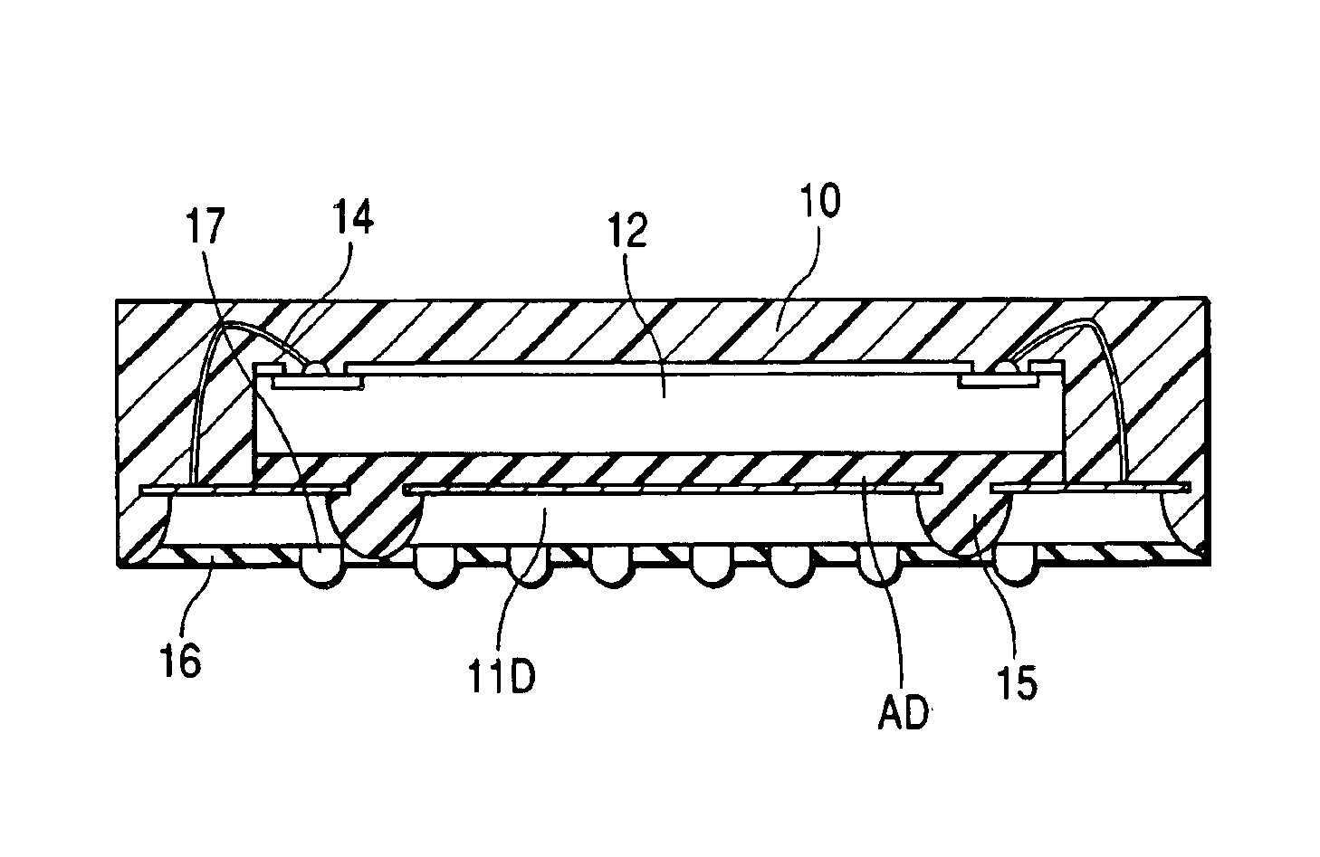
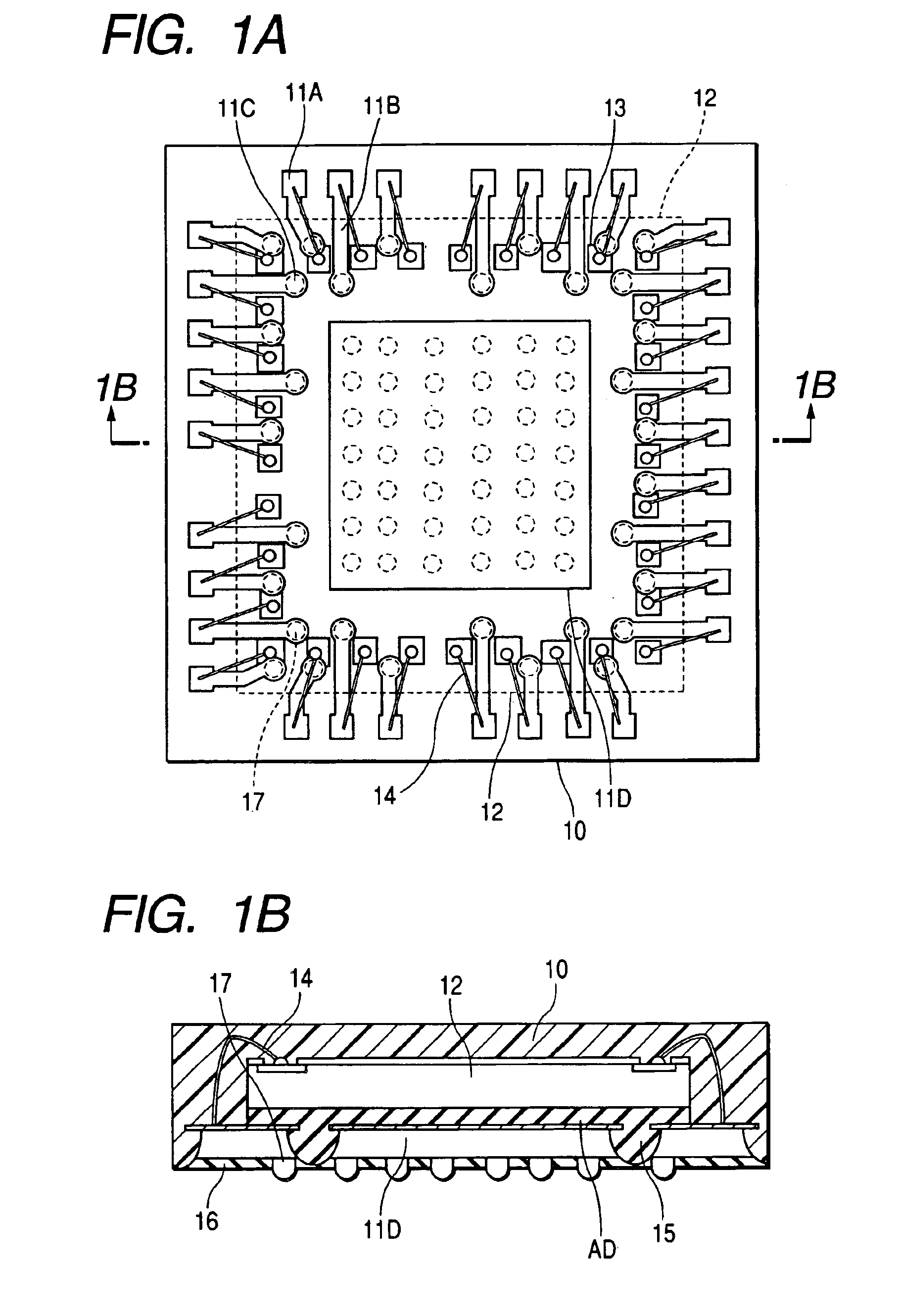
[0105]First, a semiconductor device of the invention is described referring to FIG. 1. FIG. 1A is a plan view of the semiconductor device, and FIG. 1B is a section view cut with A—A line.
[0106]FIG. 1 shows a insulating resin 10 buried with the following chips. They are pads 11A, conductive paths 11B in one body with the pads 11A, external connection electrodes 11C provided at the other ends of the conductive paths 11B in one body with the conductive paths 11B. Further an electrode for radiating 11D provided at one area surrounded by the conductive patterns 11A, 11B, and 11C and a semiconductor chip 12 provided on the electrode for radiating 11D are buried. The semiconductor chip 12 is fixed to the electrode for radiating 11D through a insulating adhesion means AD, and is shown with dotted line in FIG. 1A.
[0107]A bonding electrode 13 of the semiconductor chip 12 and the pad 11A are electrically connected through a bonding wire 14.
[0108]Side face of said conduc...
second embodiment
[0117](Second Embodiment)
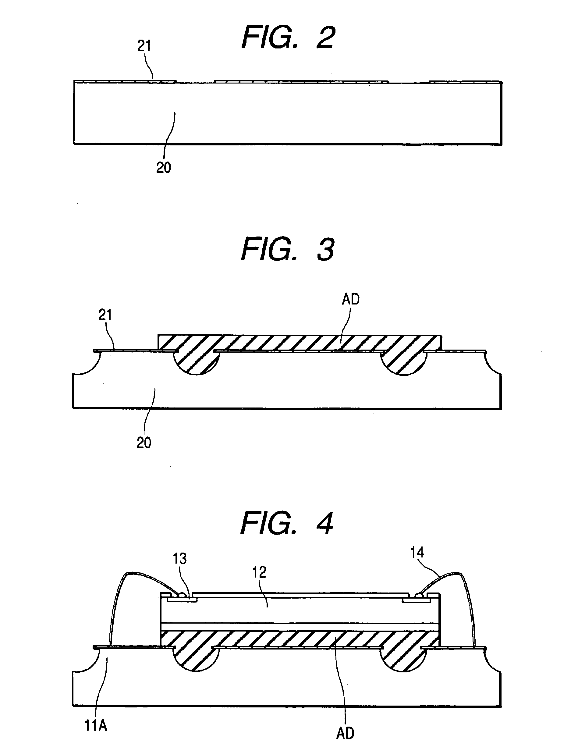
[0118]The method for manufacturing shows the method for manufacturing of the semiconductor chip 15 shown in FIG. 1, and FIG. 2 to FIG. 6 are section views corresponding to A—A line of FIG. 1A.
[0119]First, a conductive foil 20 is provided as FIG. 2. Thickness thereof is desirably 10 μm to 300 μm, here rolled copper foil of 70 μm is used. Next on the front face of the conductive foil 20, a conductive film 21 or a photo resist is formed as etching-resist.
[0120]The pattern is same pattern as the pads 11A in FIG. 1A, the conductive paths 11B, the external connection electrode 11C, and the electrodes for radiation 11D. In the case of using the photo resist instead of the conductive film 21, a conductive film such as Au, Ag, Pd or Ni is formed at a part corresponding to at least pad in the lower layer of the photo resist. This is provided to make bonding possible. (Refer FIG. 2 about the above.)
[0121]Next, a conductive foil 20 is half-etched through said conductive...
third embodiment
[0149](Third Embodiment)
[0150]FIG. 8 shows the semiconductor device 42. FIG. 8A is a plan view of the device, and FIG. 8B is a section view cut by A—A line.
[0151]Although the pad 11A is formed in one body with the conductive path 11B and the external connection electrode 11C in FIG. 1, here the back face of the pad 11A becomes the external connection electrode.
[0152]As the back face of the pad 11A is formed in rectangle, the pattern exposing from the insulating film 16 is formed in same pattern as said rectangle. The trenches 43 are formed so that the electrode 11D for radiation and chip 12 can be adhered appropriately by filling the insulating adhesion means into said trenches. Thereby the electrode 11D for radiation is divided to plural.
[0153]As clear from the above description, in the invention, even the conductive foil (or conductive foil) where the conductive pattern formed in island shape has thickness is buried in the insulating adhesion means and the insulating resin. As the...
PUM
 Abstract
Description
Claims
Application Information
 - R&D
- Intellectual Property
- Life Sciences
- Materials
- Tech Scout
- Unparalleled Data Quality
- Higher Quality Content
- 60% Fewer Hallucinations
Browse by: Latest US Patents, China's latest patents, Technical Efficacy Thesaurus, Application Domain, Technology Topic, Popular Technical Reports.
© 2025 PatSnap. All rights reserved.Legal|Privacy policy|Modern Slavery Act Transparency Statement|Sitemap|About US| Contact US: help@patsnap.com


