Plasma processing method and apparatus

a processing method and apparatus technology, applied in the field ofplasma processing methods and apparatuses, can solve problems such as difficulty in securing demandable capacitances, and achieve the effect of stable etching ra

Inactive Publication Date: 2005-06-14
PANASONIC CORP
View PDF3 Cites 9 Cited by
  • Summary
  • Abstract
  • Description
  • Claims
  • Application Information

AI Technical Summary

Benefits of technology

[0011]The present invention having been accomplished in view of these and other prior-art issues, an object of the present invention is to provide a plasma processing method and apparatus capable of achieving uniform plasma processing and ensuring a stable etching rate.

Problems solved by technology

For example, in the field of semiconductor memories (storage devices), although countermeasures for increases in the capacitance of memory capacitors have hitherto been given by changing the memory capacitor structure, it has become difficult to secure demanded capacitances only by the structure change with progress of miniaturizing.

Method used


Image

  • Plasma processing method and apparatus
  • Plasma processing method and apparatus
  • Plasma processing method and apparatus

Examples


first embodiment

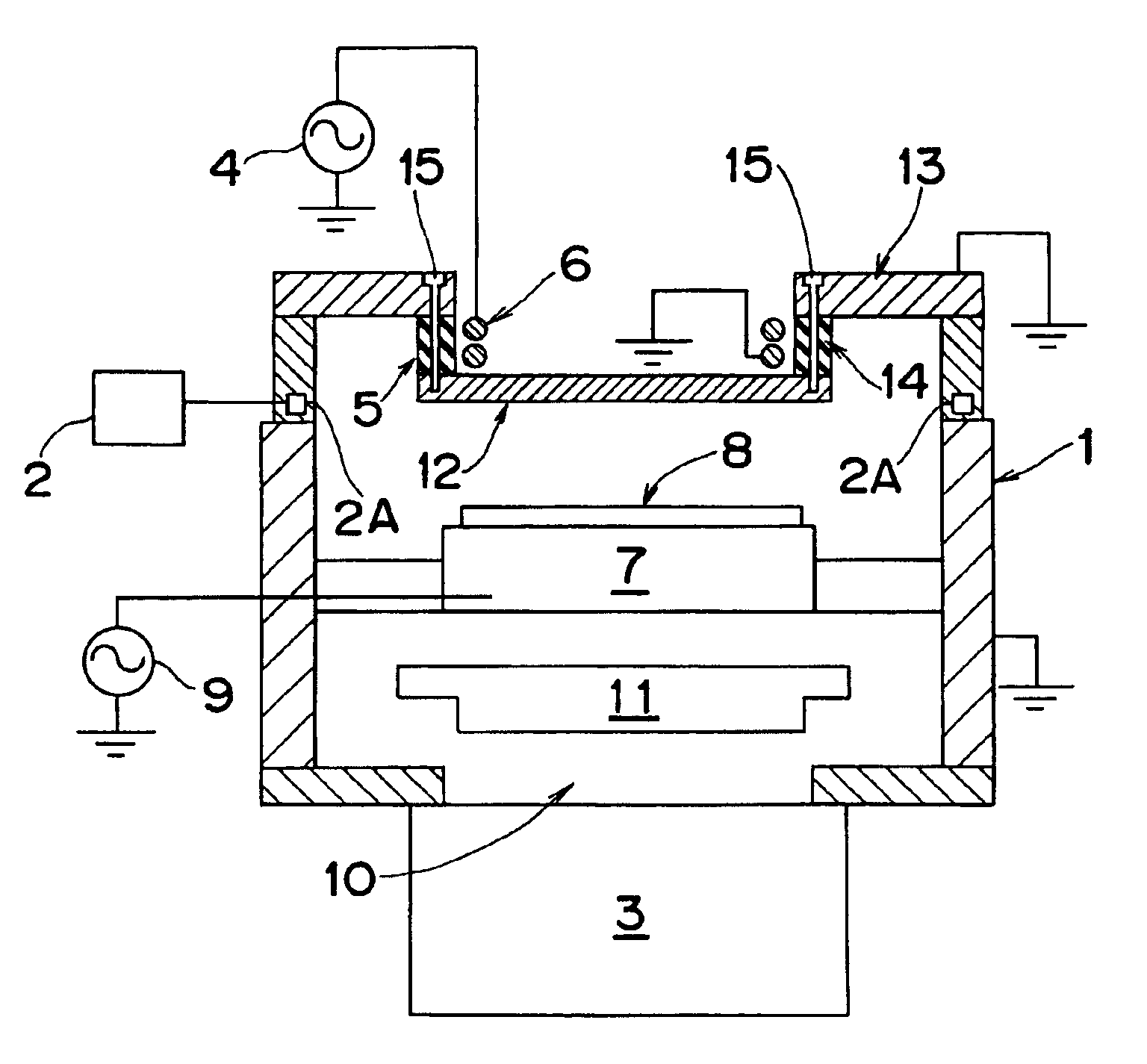
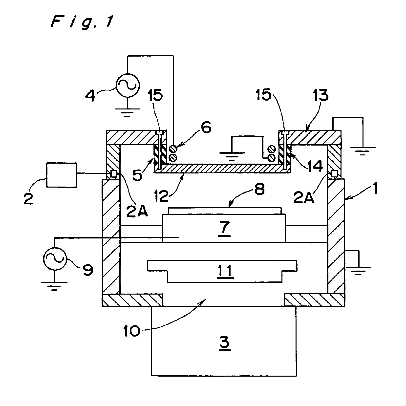
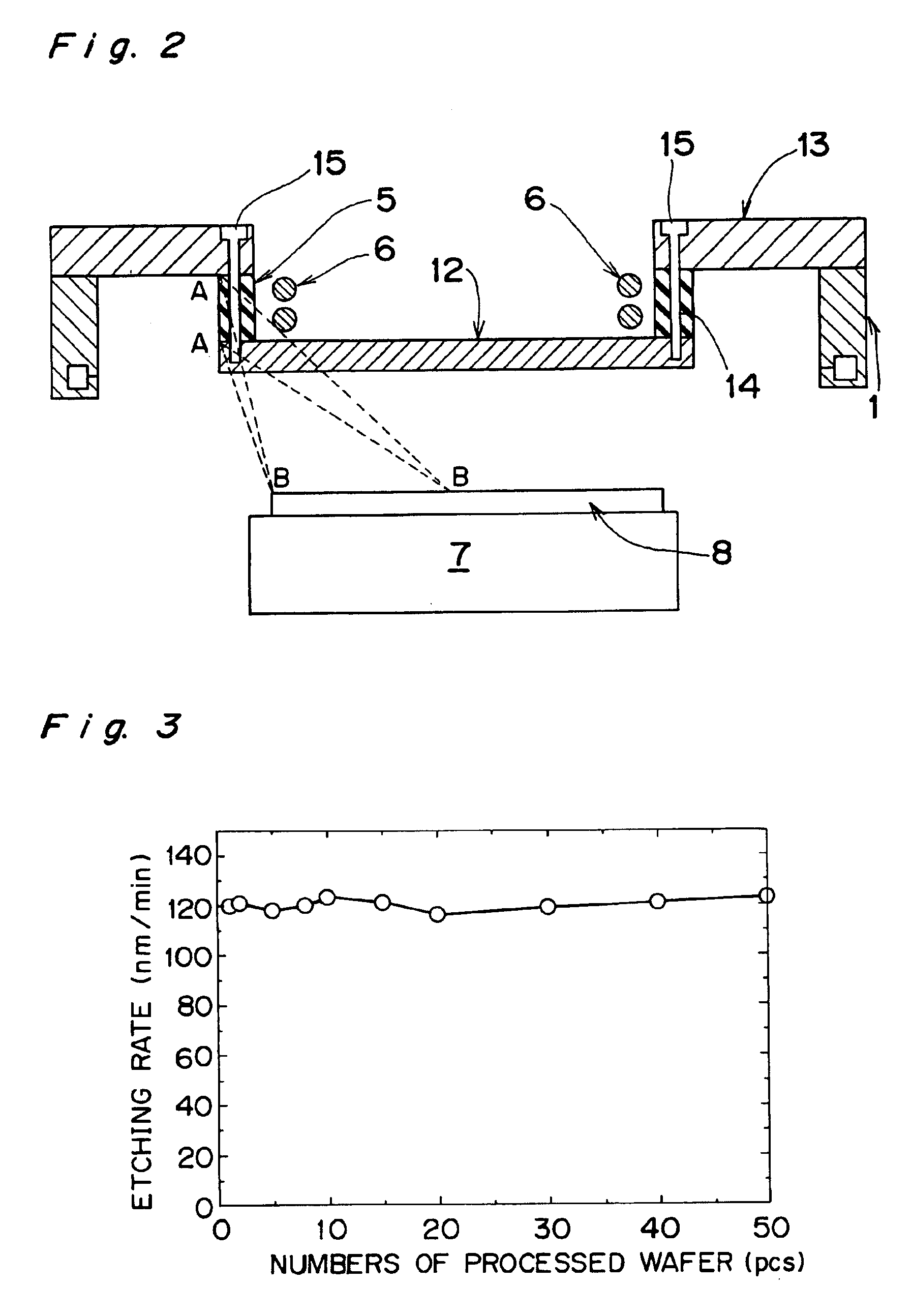
[0053]Hereinbelow, the present invention is described with reference to FIGS. 1 to 3 and 10.

[0054]FIG. 1 shows a sectional view of an etching apparatus as an example of a plasma processing apparatus used in a first embodiment of the present invention. Referring to FIG. 1, while a vacuum chamber 1 is maintained at a specified internal pressure by exhausting the vacuum chamber 1 with a turbo-molecular pump 3 serving as an exhauster and simultaneously supplying a specified gas from nozzles 2A of gas supply equipment 2 into the vacuum chamber 1, a high-frequency power of 13.56 MHz is supplied by means of coil-use high-frequency power supply equipment 4 to a coil 6 provided inside a dielectric cylinder 5 which serves as one example of a dielectric window and is formed of glass or ceramics, such as quartz glass, alumina, aluminum nitride or silicon nitride (SiN4). Thus, plasma is generated in the vacuum chamber 1, allowing the etching on an object such as a substrate 8 or a thin film ther...


PUM

PropertyMeasurementUnit
pressureaaaaaaaaaa
pressureaaaaaaaaaa
frequencyaaaaaaaaaa

Abstract

A plasma processing method includes exhausting the interior of a vacuum chamber while supplying gas into the vacuum chamber, and while maintaining the interior of the chamber at a desired pressure. A high-frequency power of 100 kHz to 100 MHz is applied to a coil provided in the vicinity of a dielectric window provided so as to face a substrate placed on a substrate electrode in the vacuum Thus, plasma is generated in the vacuum chamber to process the substrate or a film on the substrate by the generated plasma while particles which tend to move straight from a surface of the substrate or from a surface of the film on the substrate toward a wall surface of the dielectric window inside the vacuum chamber are kept interrupted by a metal plate.

Description

BACKGROUND OF THE PRESENT INVENTION[0001]The present invention relates to a plasma processing method and apparatus, such as an etching method and apparatus, to be used for manufacture of semiconductors or other electron equipment and micromachines.[0002]For manufacture of semiconductors or other electron equipment and micromachines, demands for etching techniques related to refractory metal films have been increasing year after year.[0003]For example, in the field of semiconductor memories (storage devices), although countermeasures for increases in the capacitance of memory capacitors have hitherto been given by changing the memory capacitor structure, it has become difficult to secure demanded capacitances only by the structure change with progress of miniaturizing. Due to this, ceramic base oxides having high dielectric constants such as barium / strontium titanate, lead zirconium titanate, and bismuth / strontium tantalate have come to be used as materials for capacitor capacitance....

Claims


Application Information

Patent Timeline
Patent Type & Authority Patents(United States)
IPC IPC(8): C30B33/00C30B33/12H01J37/32C23F4/00H01L21/28H01L21/302H01L21/3065H01L21/3213H01L21/8242H01L21/8246H01L27/105H01L27/108
CPCH01J37/321C30B33/12
Inventor OKUMURA, TOMOHIROKAI, TAKAYUKIYASHIRO, YOICHIRO
Owner PANASONIC CORP
Why Eureka
Try Eureka