Passband flattened demultiplexer employing segmented reflectors and other devices derived therefrom
a demultiplexer and segmented reflector technology, applied in the direction of optics, instruments, light guides, etc., can solve the problems of limiting the number of channels within the system, all limitations and drawbacks, and the type of device is not easily produced in a maimer that is commercially viabl
- Summary
- Abstract
- Description
- Claims
- Application Information
AI Technical Summary
Benefits of technology
Problems solved by technology
Method used
Image
Examples
first embodiment
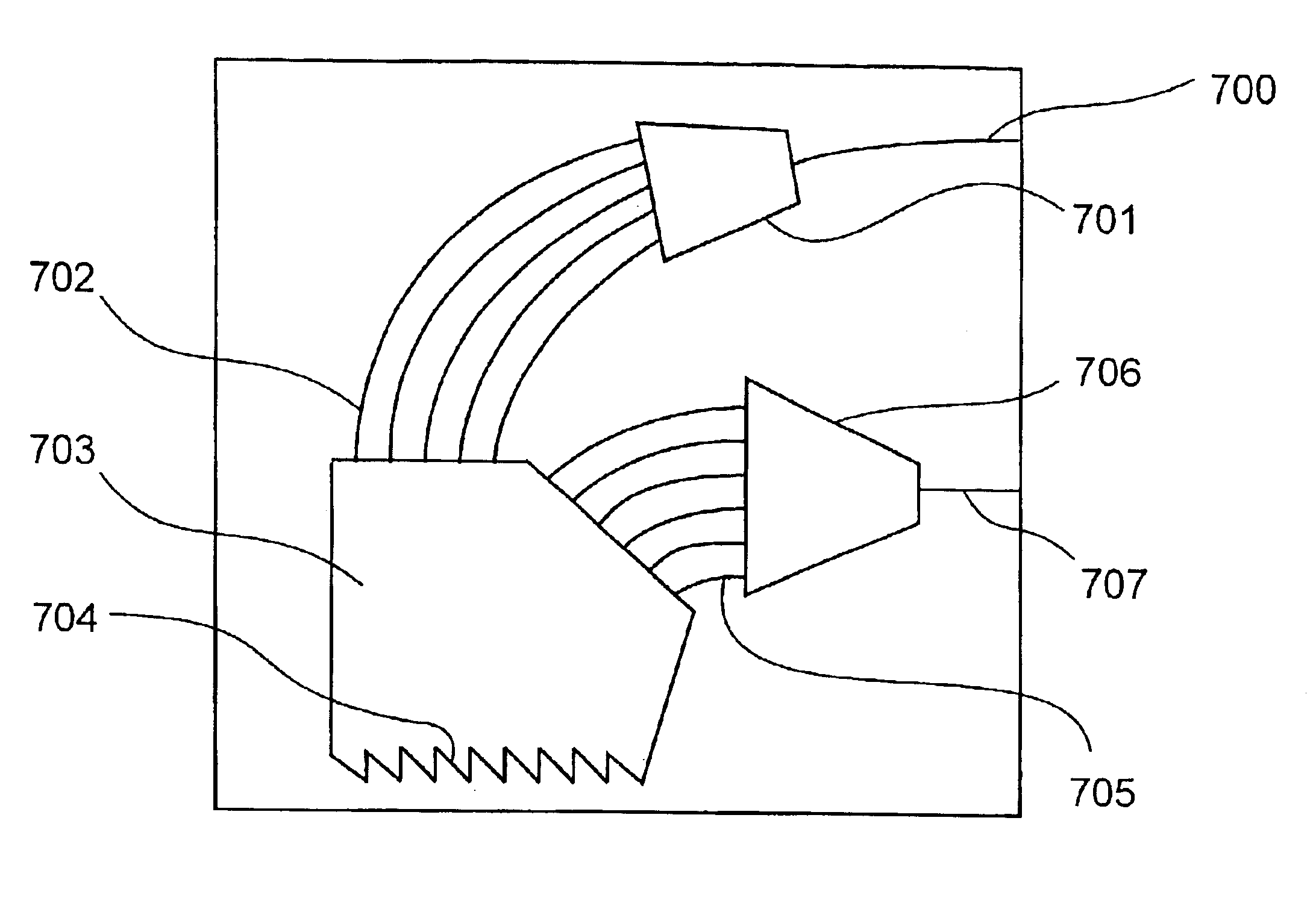
[0040]Referring to FIG. 7, a top view of the invention is shown. This embodiment features an input waveguide 700, an input slab 701, a first array of waveguides 702 and an intermediate slab region 703, a mirror array 704, a second array of waveguides 705, an output slab 706 and an output waveguide 707. This embodiment is useable as a filter for reducing the optical intensity of any optical noise present between predetermined wavelength channels. In operation, an optical signal propagates within the input waveguide 700 and through the input slab 701 into the first array of waveguides 702. The optical signal is then provided to the intermediate slab region 703 where it interacts with the mirror array 704. The mirror array 704 reflects only those portions of the optical signal that correspond to a predetermined set of wavelength channels. Thus, optical signals that do not correspond to the predetermined wavelength channels are attenuated. The remaining optical signals are reflected fro...
second embodiment
[0041]Referring to FIG. 8, the invention is shown featuring, an input waveguide 800, an input slab 801, a first array of waveguides 802, an intermediate slab 803, an array of adjustable mirrors 804, a second array of waveguides 805, a first output slab 806, a first set of output ports 807, a third array of waveguides 808, a second output slab 809 and a second set of output ports 810. In this embodiment, a wavelength multiplexed optical signal is provided to the input waveguide 800 and propagates to the input slab 801 where it is coupled to the first array of waveguides 802. The wavelength multiplexed optical signal propagates within the intermediate slab region 803 and focuses on the array of adjustable mirrors 804. The device is designed such that the optical signals corresponding to predetermined wavelength channels are provided to specific mirrors of the array of adjustable mirrors 804. Optical signals corresponding to gaps between the predetermined wavelength channels are attenu...
third embodiment
[0042]Referring to FIG. 9, the invention is shown. The function and description of elements shown in FIG. 9 are equivalent to elements of other figures having the same reference numerals. An intermediate waveguide 907 receives a multiplexed optical signal from the output slab 706. The multiplexed optical signal propagates to the demultiplexer input slab 908. Portions of the multiplexed optical signal then propagate along the demultiplexer array of waveguides 909 and are received by the demultiplexer output slab 910. A set of optical signals is provided to the array of output waveguides 911. The geometry and physical properties of the structure are chose such that each of the optical signals present in array of output waveguides 911 corresponds to a predetermined wavelength channel. Thus, this embodiment of the invention receives an multiplexed optical signal, filters the signal and then separates the filtered multiplexed optical signal into a set of optical signals each optical sign...
PUM
 Abstract
Description
Claims
Application Information
 - R&D
- Intellectual Property
- Life Sciences
- Materials
- Tech Scout
- Unparalleled Data Quality
- Higher Quality Content
- 60% Fewer Hallucinations
Browse by: Latest US Patents, China's latest patents, Technical Efficacy Thesaurus, Application Domain, Technology Topic, Popular Technical Reports.
© 2025 PatSnap. All rights reserved.Legal|Privacy policy|Modern Slavery Act Transparency Statement|Sitemap|About US| Contact US: help@patsnap.com


