Electronic device, method of manufacturing the same, metal particle, and electroconductive paste

a manufacturing method and electroconductive technology, applied in the direction of semiconductor devices, semiconductor/solid-state device details, electrical apparatus, etc., can solve the problems of kirkendall void generation, mechanical strength degradation, reliability and quality degradation of bonded parts and conductors, etc., to achieve high mechanical strength, less likely to cause separation, disconnection or separation

Active Publication Date: 2016-12-06
NAPRA
View PDF24 Cites 2 Cited by
  • Summary
  • Abstract
  • Description
  • Claims
  • Application Information

AI Technical Summary

Benefits of technology

[0010]It is therefore an object of this invention to provide an electronic device having a conductor which has a high bond strength, a high mechanical strength, and is less likely to cause separation, disconnection or the like; a method of manufacturing such electronic device; and a metal particle and an electroconductive paste suitable for the method of manufacturing the electronic device.

Problems solved by technology

Another known problem intrinsic to diffusion bonding of metal relates to degradation in mechanical strength due to Kirkendall void.
The Kirkendall void generates when atomic vacancies (lattice defects), caused by unbalanced mutual diffusion, accumulate without disappearing.
The Kirkendall void grows up to a larger void or crack to degrade reliability and quality of the bonded part and the conductor, and to further degrade the mechanical strength, which may even result in separation, disconnection or the like.
A similar problem would occur when the connection parts, which mutually connect the semiconductor chips, are formed on the surface of a wafer, in electric interconnect making use of through-conductor, electric interconnect making use of planar conductor pattern, and in electronic devices in the form of three-dimensional system-in-package (3D-SiP).

Method used


Image

  • Electronic device, method of manufacturing the same, metal particle, and electroconductive paste
  • Electronic device, method of manufacturing the same, metal particle, and electroconductive paste
  • Electronic device, method of manufacturing the same, metal particle, and electroconductive paste

Examples


Embodiment Construction

1. Electronic Device

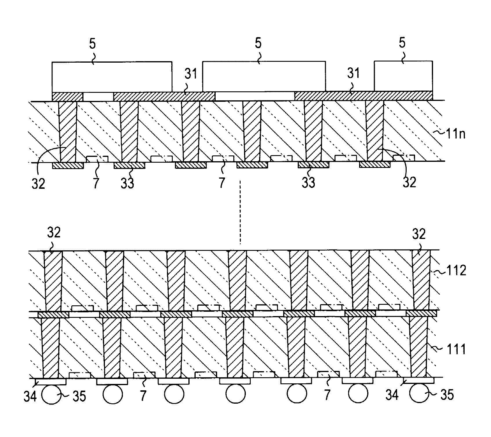
[0041]The electronic device of this invention has, as illustrated in FIG. 1, conductors 31 which allow an electric signal to transmit therethrough. The conductors 31 are formed on the surface of a substrate 111. The substrate 111 may be composed of a semiconductor substrate, organic insulating substrate, inorganic insulating substrate, electroconductive substrate with an insulating coverage, or, composite substrate or stacked substrate composed of them.

[0042]The conductors 31 may only be a substance which allows an electric signal to transmit therethrough, and includes electrode, interconnect, bump, bonding conductor and so forth. In the example illustrated in FIG. 1, the conductors 31 configure electrodes, interconnects or bumps.

[0043]FIG. 2 illustrates another embodiment of the electronic device according to this invention. In this embodiment, illustrated is a three-dimensional electronic device in which a plurality of (n) substrates 111 to 11n are stacked one ...


PUM

PropertyMeasurementUnit
particle sizeaaaaaaaaaa
sizesaaaaaaaaaa
particle sizeaaaaaaaaaa

Abstract

Provided is an electronic device which includes a conductor allowing an electric signal to transmit therethrough, the conductor containing a plurality of species of metal components having different melting points, and internally having a constituent concentration gradient produced as a result of diffusion of the metal components.

Description

BACKGROUND OF THE INVENTION[0001]1. Field of the Invention[0002]This invention relates to an electronic device, a method of manufacturing the same, and a metal particle and an electroconductive paste which are suitable for the method of manufacturing.[0003]2. Description of the Related Art[0004]In the field of electronic devices including integrated circuits of a variety of scales, various semiconductor elements or chips thereof, there has been proposed a technique of obtaining a three-dimensional circuit arrangement, called TSV (Through-Silicon-Via), by which a large number of through-conductors are preliminarily provided to each of circuit boards, the circuit boards are stacked and bonded. The three-dimensional circuit arrangement, applied with the TSV technique, will have a large number of functions integrated into a small occupation area. In addition, it also becomes possible to accelerate the processing speed, since principal electric interconnects among the elements can be dra...

Claims


Application Information

Patent Timeline
Patent Type & Authority Patents(United States)
IPC IPC(8): H01L23/48H01L23/00
CPCH01L24/32H01L2224/32235H01L2924/3656H01L2224/32505H01L2224/29009H01L2224/29644H01L2224/29655H01L2224/29664H01L2224/29671H01L21/76898H01L24/11H01L24/13H01L24/16H01L24/27H01L24/29H01L24/81H01L24/83H01L2224/1132H01L2224/13009H01L2224/16505H01L2224/2732H01L2224/2929H01L2224/293H01L2224/81862H01L2224/83851H01L2224/83862H01L2224/2957H01L2224/29561H01L2224/296H01L2224/29613H01L2224/29657H01L2224/29669H01L23/481H01L23/53233H01L23/49827H01L23/49883H01L23/147H01L2924/013H01L2924/00014
Inventor SEKINE, SHIGENOBU
Owner NAPRA
Why Eureka
Try Eureka