Encapsulated Circuit Module, And Production Method Therefor

a technology of circuit modules and circuits, applied in the direction of semiconductor devices, semiconductor/solid-state device details, electrical apparatus, etc., can solve the problems of electromagnetic waves, electromagnetic waves, and other electronic components being vulnerable to electromagnetic waves,

Active Publication Date: 2017-11-30
MEIKO ELECTRONICS CO LTD
View PDF18 Cites 3 Cited by
  • Summary
  • Abstract
  • Description
  • Claims
  • Application Information

AI Technical Summary

Benefits of technology

[0019]On the other hand, in the present invention, the surface of the first resin is further covered with the second resin. The second resin does not contain filler. In the present invention, the shield layer which is a metal layer electrically connected with the ground electrode is formed on the surface of the second resin and the side surfaces of the second resin, the first resin and the substrate exposed by the snicking step performed before the snipping for dicing. The second resin does not contain filler as described above. The shield layer thus formed does not have a problem of falling off which otherwise can occur due to the falling off of the filler.
[0020]Even in the method of the present application, the portion of the shield layer that covers the side surface of the first resin covers the first resin without the interposed second resin. The present inventor has found, however, that the side surface of the first resin is roughened appropriately as a result of the snicking step performed in an ordinary method and that the shield layer adheres to the first resin well and is thus less likely to be separated.

Problems solved by technology

Some electronic components are vulnerable to electromagnetic waves.
Moreover, some other electronic components are vulnerable to electromagnetic waves and others emit electromagnetic waves.
When, however, a box is used, the height from the substrate to the upper surface of the box often becomes relatively great, and the thickness of the circuit module thus tends to be great.
Where boxes are used, it takes time and cost to make these boxes.
Different kinds of boxes, if prepared depending on the height of electronic components, further increase the process steps and costs required for making the boxes.
As a result, the height of the box may possibly be unnecessarily great relative to the height of the electronic component(s) on the substrate.
Boxes, however, often increase the thickness of the circuit module.

Method used


Image

  • Encapsulated Circuit Module, And Production Method Therefor
  • Encapsulated Circuit Module, And Production Method Therefor
  • Encapsulated Circuit Module, And Production Method Therefor

Examples


Embodiment Construction

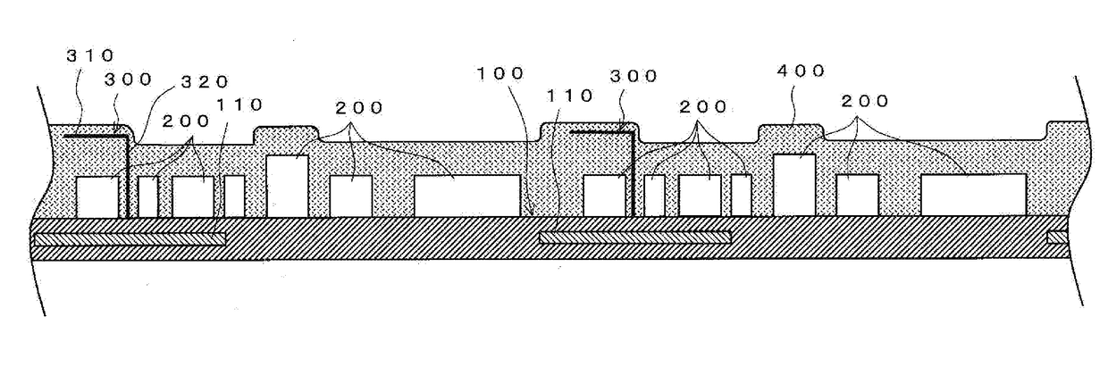
[0024]As described above, according to the present invention, at least the portion of the upper surface of the first resin covered with the shield layer is covered with the second resin, which prevents the shield layer from falling off due to falling off of the filler. In the present invention, however, since the shield layer is formed on the first resin with the second resin interposed therebetween, when the second resin falls off from the first resin, the shield layer falls off accordingly.

[0025]In order to prevent the second resin from falling off from the first resin, adhesion of the second resin to the first resin is important. This adhesion is achieved by an anchor effect, an intermolecular force, and some covalent bond between the first resin and the second resin.

[0026]In order to improve the adhesion of the second resin to the first resin, it is easy to use a same type of resin as that contained as a major resin component in the first resin as the second resin. In the presen...


PUM


Abstract

To provide a technique of preventing, in an encapsulated circuit module having a metal shield layer covering a surface of a resin layer containing filler, the shield layer from falling off.
In manufacturing encapsulated circuit modules, first, a substrate 100 is covered with a first resin 400 containing filler together with an electronic component 200. Next, a surface of the first resin 400 is covered with a second resin 500 containing no filler. Subsequently, a ground electrode 110 in the substrate 100 is exposed by snicking and then a shield layer 600 that covers the entire surface of the substrate 100 is formed by electroless plating. Thereafter, snipping is performed to obtain a number of encapsulated circuit modules.

Description

TECHNICAL FIELD[0001]The present invention relates to encapsulated circuit modules.BACKGROUND ART[0002]Encapsulated circuit modules are known.[0003]Encapsulated circuit modules include a substrate having wiring (such as a printed wiring board), electronic components mounted so as to be electrically connected with the wiring of the substrate, and a resin covering the substrate together with the electronic components. By covering the electronic components with the resin, encapsulated circuit modules can provide protection for electronic components and protection of electrical contacts between the electronic components and the wiring of the substrate.[0004]Encapsulated circuit modules include electronic components as described above. Some electronic components are vulnerable to electromagnetic waves. Other electronic components emit electromagnetic waves.[0005]In many situations where an encapsulated circuit module is actually used, the encapsulated circuit module is combined with othe...

Claims


Application Information

Patent Timeline
Patent Type & Authority Applications(United States)
IPC IPC(8): H01L23/00H01L23/29H01L21/67H01L21/56H05K9/00H01L23/31
CPCH01L24/97H01L23/3121H01L23/29H01L2924/3025H01L21/6715H05K9/0088H01L2924/1815H01L21/56H01L21/561H01L23/552H01L23/66H01L2223/6677
Inventor MIWA, SATORU
Owner MEIKO ELECTRONICS CO LTD
Why Eureka
Try Eureka