
On-chip capacitor

a capacitor and chip technology, applied in the field of integrated circuit structures, can solve the problems of increasing the functional complexity of the integrated circuit as a whole, reducing the speed of ics, and thus the speed, and reducing the efficiency of ics, so as to increase the intralevel or “sidewall” capacitance of the whole structure, eliminate the contribution of top-bottom capacitance, and increase the intralevel capacitance

Inactive Publication Date: 2005-05-24
TEXAS INSTR INC
View PDF14 Cites 37 Cited by
  • Summary
  • Abstract
  • Description
  • Claims
  • Application Information

AI Technical Summary

Benefits of technology

The present invention is about making integrated circuits with on-chip capacitors. The technical effect is that this invention helps to make more efficient and effective integrated circuits.

Problems solved by technology

This objective has caused integrated circuit fabrication to seek ways of scaling down devices, increasing the functional complexity of the integrated circuit as a whole.
However, downscaling of ICs, and therefore speed, is limited by interconnect technology.
One problem with multi-level interconnect structures is the filling of high aspect ratio and varying depth contact holes and vias.
Another problem is the tendency of closely situated conductors to crosstalk, where potential change in one line affects performance of a nearby line.

Method used


Image

  • On-chip capacitor
  • On-chip capacitor
  • On-chip capacitor

Examples


Embodiment Construction

[0031]The numerous innovative teachings of the present application will be described with particular reference to the presently preferred embodiment. However, it should be understood that this class of embodiments provides only a few examples of the many advantageous uses of the innovative teachings herein. In general, statements made in the specification of the present application do not necessarily delimit any of the various claimed inventions. Moreover, some statements may apply to some inventive features but not to others.

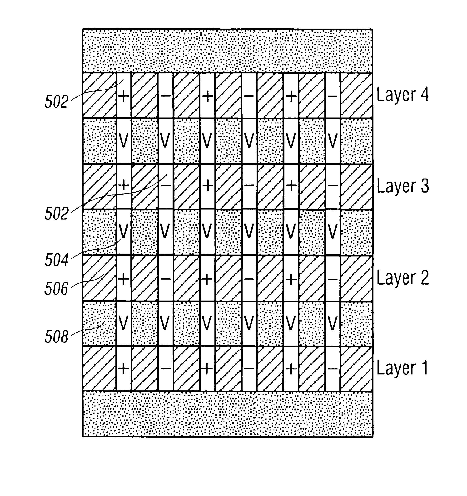
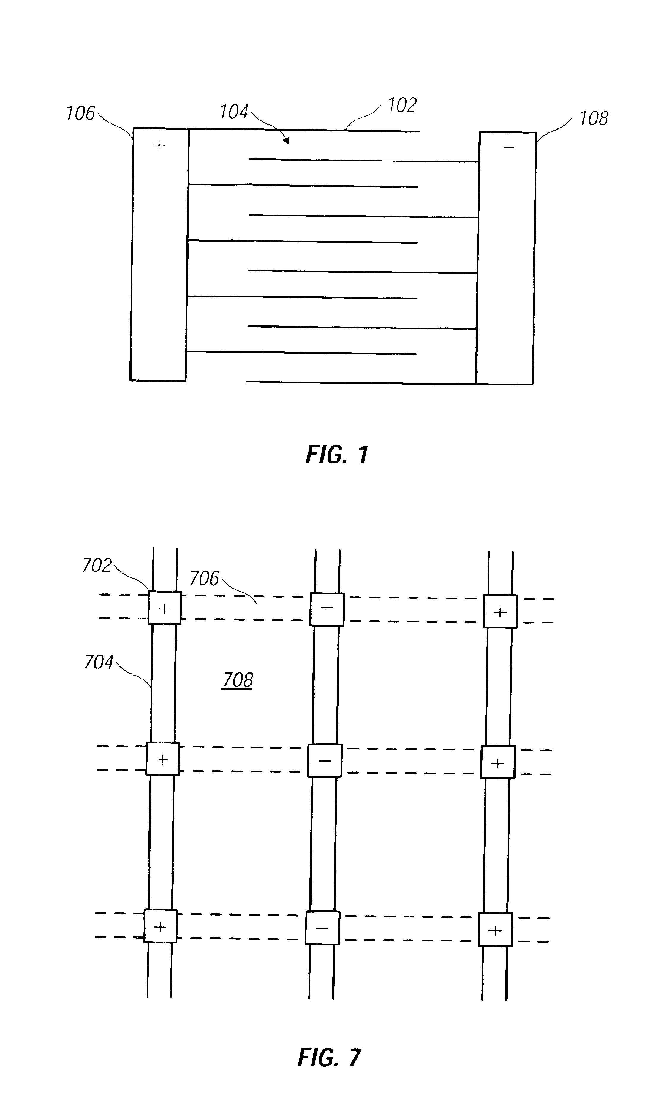
[0032]The preferred embodiment is described with reference to the figures. FIG. 1 shows the top view of an interconnect layer in a CMOS process. Metallization lines 102 are located in close proximity to one another separated by dielectric material 104. Lines of like polarity are connected to a common bus. FIG. 1 shows two busses 106, 108. For purposes of discussion, one bus 106 is labeled “+” while the other 108 is labeled “−”. The potential difference between ...


PUM


Abstract

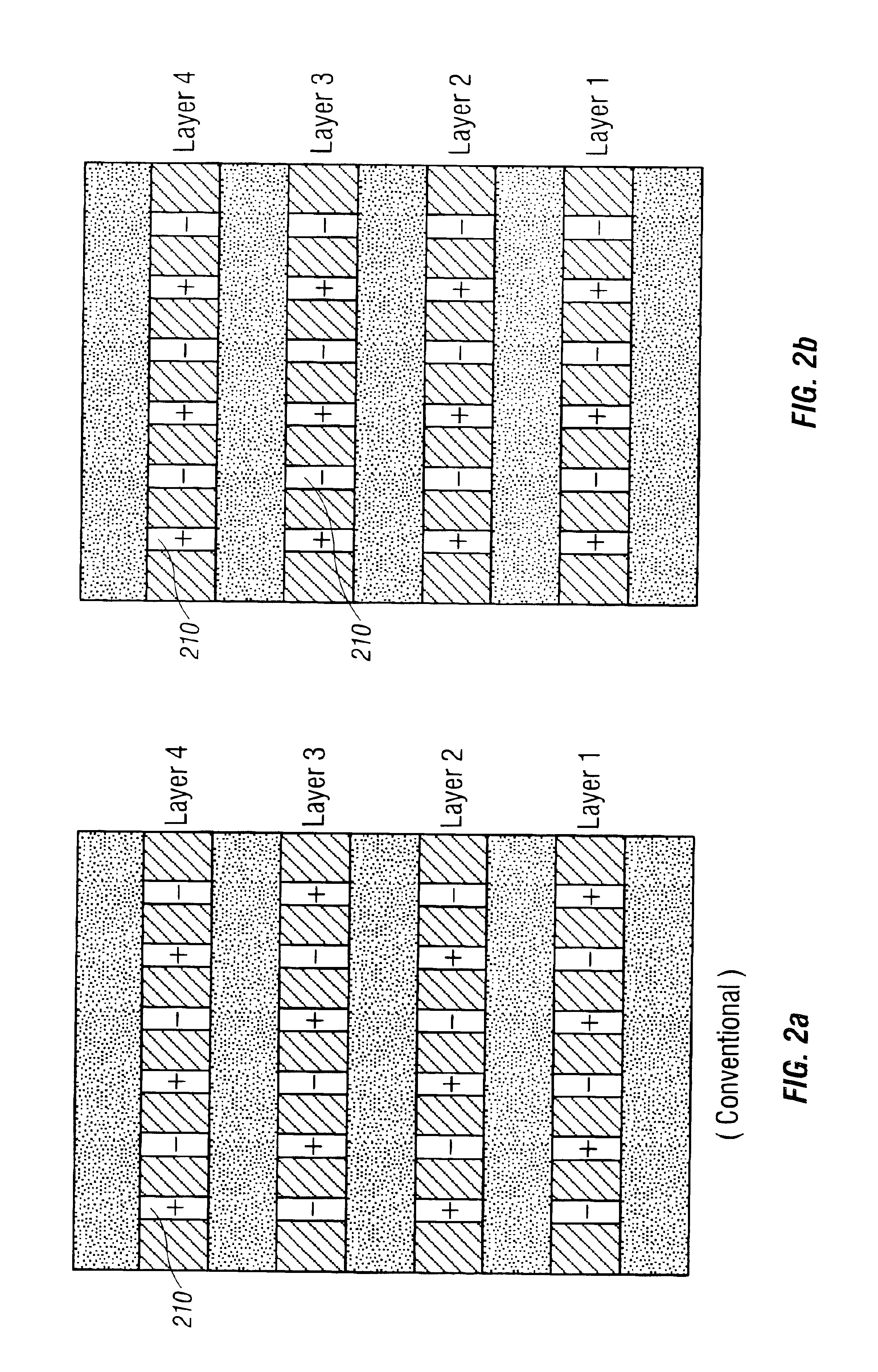
An on-chip analog capacitor. Metal interconnect structures are used to form the capacitor, and the interdigitated fingers of like polarity within the interconnect structure are connected above and below to one another by metal vias to form a wall of metal which increases total capacitance by taking advantage of the via sidewall capacitance.

Description

[0001]This application is a continuation of Ser. No. 09 / 935,519 filed Aug. 23, 2001 now U.S. Pat. No. 6,635,916, which claims benefit of Ser. No. 60 / 229,488 filed Aug. 31, 2000.BACKGROUND AND SUMMARY OF THE INVENTION[0002]The present invention relates to integrated circuit structures, and particularly to on-chip capacitors.BACKGROUND[0003]In integrated circuit fabrication, many devices are placed on a single substrate. The various devices must be electrically isolated from one another, but some specific devices must be electrically interconnected to implement a desired circuit function. Many circuits require more than one level of interconnect, so multi-level interconnect structures are used.[0004]One aim of integrated circuit technology is an increase in device speed. This objective has caused integrated circuit fabrication to seek ways of scaling down devices, increasing the functional complexity of the integrated circuit as a whole. However, downscaling of ICs, and therefore spee...

Claims


Application Information

Patent Timeline
Patent Type & Authority Patents(United States)
IPC IPC(8): H01L27/08H01L27/04H01L21/822
CPCH01L27/0805
Inventor ATON, THOMAS J.
Owner TEXAS INSTR INC
Learn More