Thin stacked package and manufacturing method thereof

a technology of integrated circuits and stacked packages, applied in the direction of semiconductor devices, semiconductor/solid-state device details, electrical apparatus, etc., can solve the problems of mcm facing poor yield, incomplete module failure test, and bare silicon chips for mcm not being tested before the chips are packaged, so as to increase the yield of stacked packages and eliminate additional leads deformation and/or treatment

Inactive Publication Date: 2005-04-12
SAMSUNG ELECTRONICS CO LTD
View PDF25 Cites 85 Cited by
  • Summary
  • Abstract
  • Description
  • Claims
  • Application Information

AI Technical Summary

Benefits of technology

Accordingly, an object of the present invention is to provide thin semiconductor stacked packages. Another object is to allow for the testing of the individual packages of the stacked package. Still another object is to increase the yield of the stacked package by eliminating additional leads deformation and / or treatment.

Problems solved by technology

Bare silicon chips for MCM cannot be tested before the chips are packaged.
And, any one chip that is not operant causes the entire module to fail test.
Thus, the MCM is faced with poor yields and little chance of rework.
In addition, that MCM technology is not commonly available to burn-in bare silicon chips; burn-in must be done at the module level.
Moreover, the stacked package needs to deform or bend the package leads in order to interconnect upper and lower packages, and thereby reduces the yield of the stacked package.

Method used


Image

  • Thin stacked package and manufacturing method thereof
  • Thin stacked package and manufacturing method thereof
  • Thin stacked package and manufacturing method thereof

Examples


first embodiment

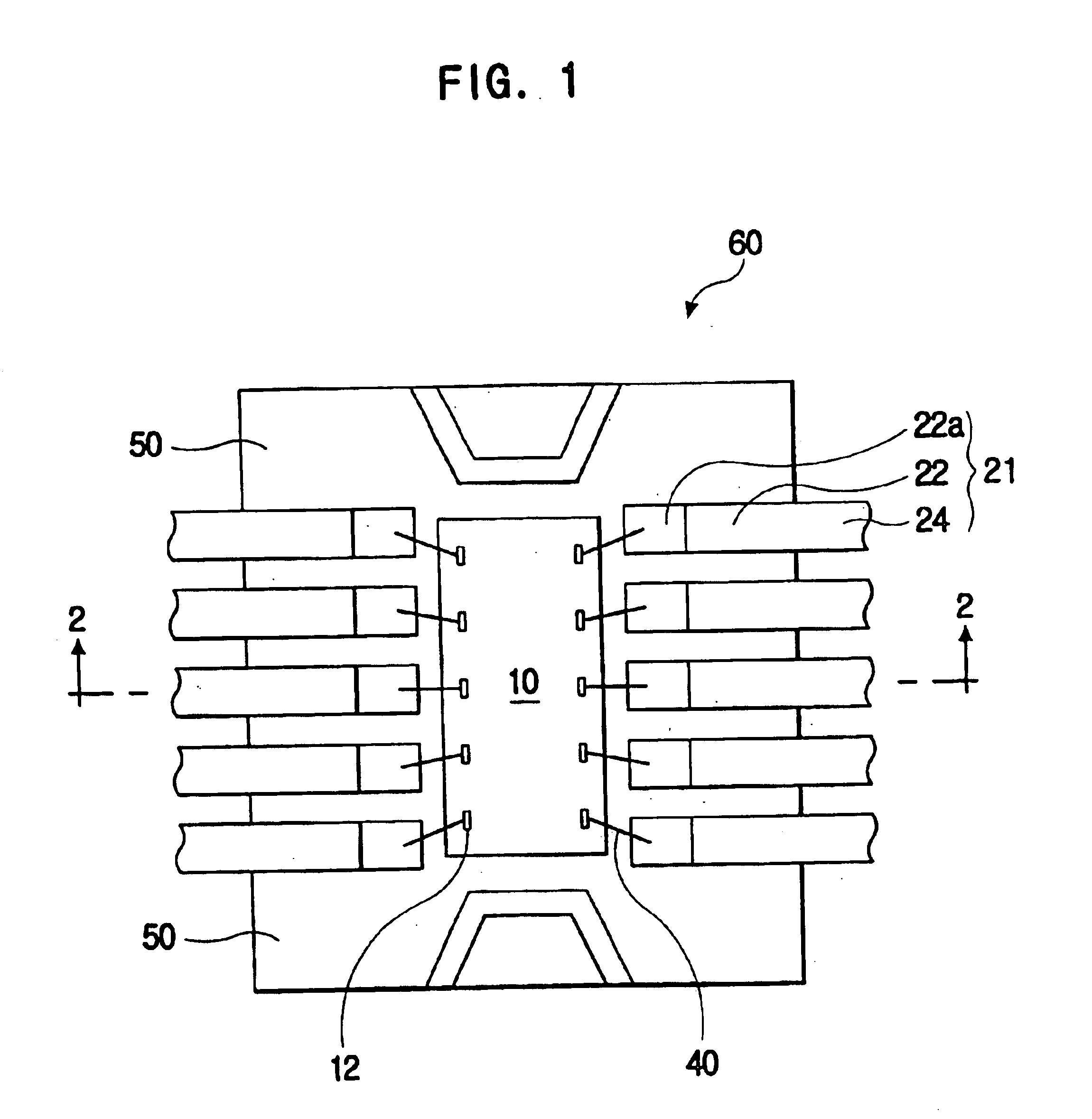
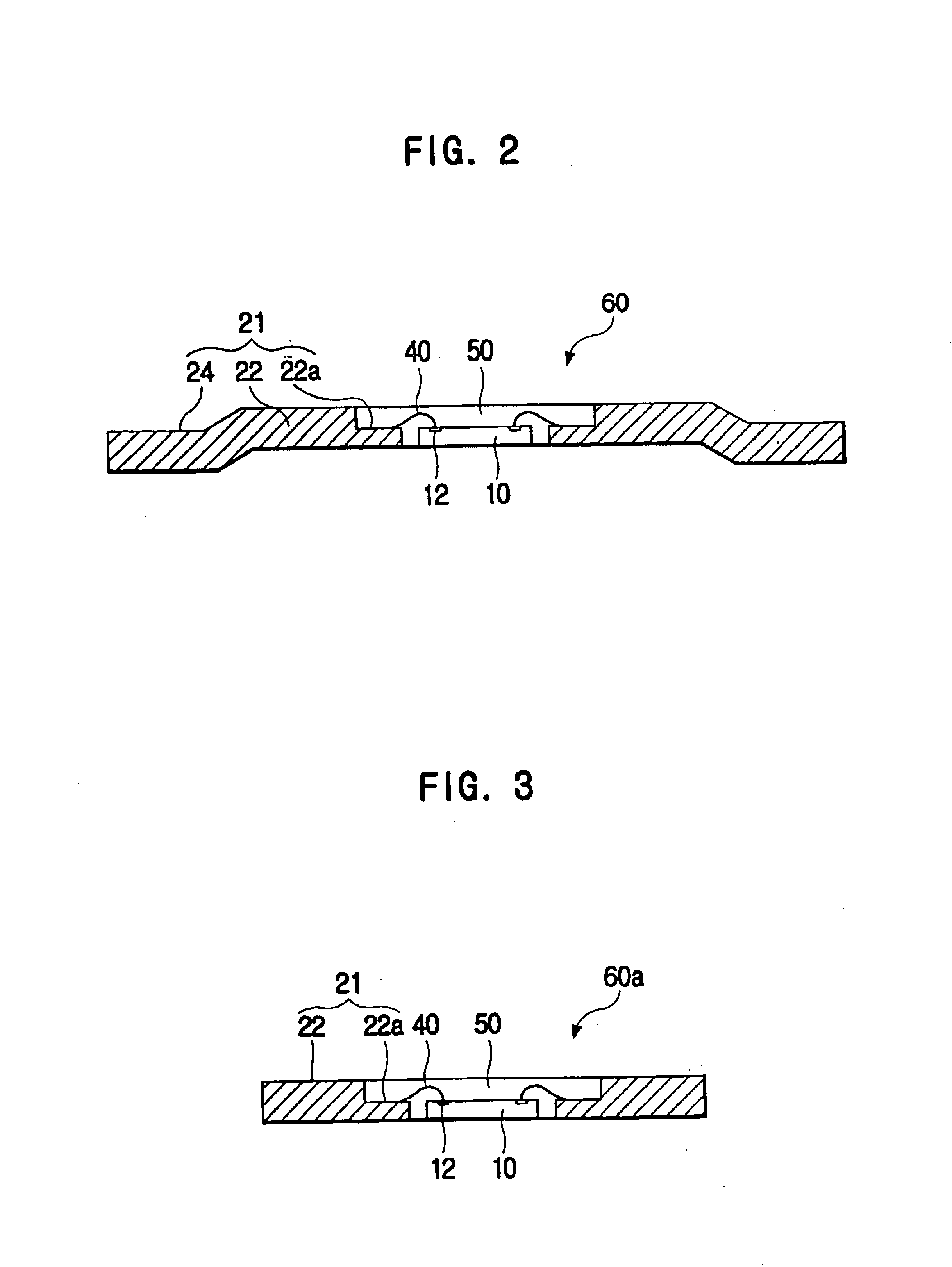
FIG. 1 is a plan view of a semiconductor device package 60 according to the present invention. FIG. 2 is a cross-sectional view, taken along the line 2—2 of FIG. 1, of the package having a plurality of outer leads to protrude from the package body and to be bent in gull-wing type.

Referring to FIGS. 1 and 2, the semiconductor device package 60 comprises a semiconductor chip 10, a plurality of leads 21 electrically connected to the semiconductor chip 10 via a metal wire 40, and a package body 50 encapsulating the semiconductor chip 10 and the metal wire 40 with a resin compound.

The semiconductor chip 10 is an edge pad type chip having a plurality of electrode pads 12 on opposite edges of its active surface. Although the current embodiment uses the edge pad type chip 10, a center pad type chip or a center and edge pads combined type chip may be used.

The leads 21 have inner leads 22 which are embedded in the package body 50, and outer leads 24 which protrude from the package body 50. Ea...

second embodiment

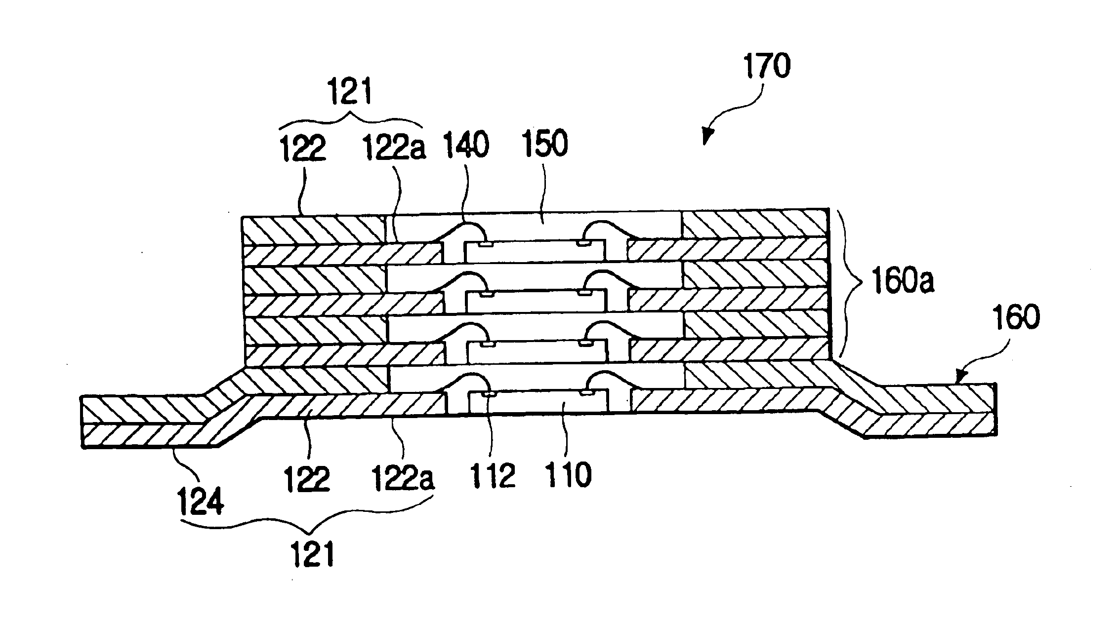
FIG. 14 shows a semiconductor device package 160 having outer leads 124 protruding from the package body 150 and bent in gull wing type according to the present invention.

With reference to FIG. 14, the semiconductor device package 160 comprises a lead frame 120 including a lower lead frame 126 and an upper lead frame 128 attached to the lower lead frame 126. The upper lead frame 128 is formed on the lower lead frame 126 except for terminal ends of the lower lead frame 162 which will be the connection terminals 122a. Other elements of the package 160 are identical with the package 60 of the first embodiment, and therefore their detailed descriptions are omitted.

According to the current embodiment, the connection terminals 122a are formed without the half-etching of the inner leads 122, and thereby the number of the manufacturing steps of the lead frame 120 can be reduced. First, the lower lead frame material is prepared. The upper lead frame material having an opening for exposing th...

third embodiment

FIG. 17 shows a semiconductor device package 260 having outer leads 224 protruding from the package body 250 and bent in gull wing type according to the present invention.

With reference to FIG. 17, the semiconductor device package 260 comprises a semiconductor chip 210 having a plurality of electrode pads 212 thereon, metal bumps 240 on the electrode pads 212, a plurality of leads 221, and a package body 250 formed by encapsulating the chip 210, the metal bumps 240, and partially the leads 221 with a liquid molding resin.

The semiconductor chip 210 is an edge pad type chip having a plurality of the electrode pads 212 on opposite two edges of the active surface, and each of the metal bumps 240 is formed the respective electrode pad 212 and connects the chip 210 to the leads 221. The metal bumps 240 are formed by the known plating or wire bonding methods.

The leads 221 comprise a plurality of inner leads 222 embedded in the package body 250, and a plurality of outer leads 224 protruding...


PUM


Abstract

There are disclosed a stacked package formed by stacking semiconductor device packages and a manufacturing method thereof. Each package includes leads and connection terminals. A semiconductor chip is electrically connected to the connection terminals. A package body has the same thickness as that of the lead so as to expose the upper and the lower surfaces of the leads to the package body. Each of the packages is stacked on another package by electrically connecting the exposed upper and lower surfaces of the leads with each other. The manufacturing method has preparing lead frames, attaching an adhesive tape to the lower surface of the lead frame, bonding a semiconductor chip to the adhesive tape in the chip receiving cavity between the leads, connecting the semiconductor chip to the connection terminals, forming a package body, removing the adhesive tape; removing dam bars from the side frame, separating packages from the lead frame, and forming a stacked package by stacking a plurality of the packages.

Description

BACKGROUND OF THE INVENTION1. Field of the InventionThe present invention generally relates to semiconductor devices and method for manufacturing the same, and more particularly to stacking structures of semiconductor integrated circuit packages and method for manufacturing the packages.2. Description of the Related ArtsIn general, semiconductor dies or chips are individually packaged for use in plastic or ceramic packages. A plurality of outer leads protruding from the package body are soldered on a supporting substrate such as a printed circuit board, or inserted into a socket. These packages, especially the packages inserted into the socket, have a large mounting area occupied on the printed circuit board.The printed circuit board is being developed toward a smaller size and a higher density, and thereby requires a higher-densely packaging technique. Therefore, a multichip module or package capable of supporting several chips on a single package, has been developed.The MCM or the...

Claims


Application Information

Patent Timeline
Patent Type & Authority Patents(United States)
IPC IPC(8): H01L21/50H01L21/44H01L21/02H01L21/48H01L23/498H01L23/31H01L23/48H01L23/495H01L23/52H01L25/10H01L29/40
CPCH01L23/3107H01L23/49537H01L23/49548H01L23/49575H01L25/105H01L2924/10253H01L2225/1064H01L2225/1029H01L24/49H01L24/48H01L2924/18165H01L2224/16H01L2224/48091H01L2224/48247H01L2224/49171H01L2924/01078H01L2924/01079H01L2924/14H01L2924/00014H01L2924/00H01L2224/451H01L2224/45124H01L2224/45144H01L24/45H01L2224/05571H01L2224/05573H01L2224/05554H01L2224/16245H01L2924/18161H01L2924/181H01L2924/10161H01L24/05H01L2924/00015H01L2224/05599H01L23/498
Inventor LYU, JU HYUNLEE, KWAN JAICHO, TAE JE
Owner SAMSUNG ELECTRONICS CO LTD
Why Eureka
Try Eureka