
Complementary Schottky junction transistors and methods of forming the same

a schottky junction transistor and junction transistor technology, applied in the field of complementary field effect transistor devices, can solve the problems of low speed, inability to improve the speed fsub>t /sub>of micropower devices by reducing the gate length lsub>g/sub>, and is not typically practical, so as to achieve faster switching speed, better transistor matching, and dramatic reduction of current requirements

Inactive Publication Date: 2005-03-08
ARIZONA STATE UNIVERSITY
View PDF26 Cites 34 Cited by
  • Summary
  • Abstract
  • Description
  • Claims
  • Application Information

AI Technical Summary

Benefits of technology

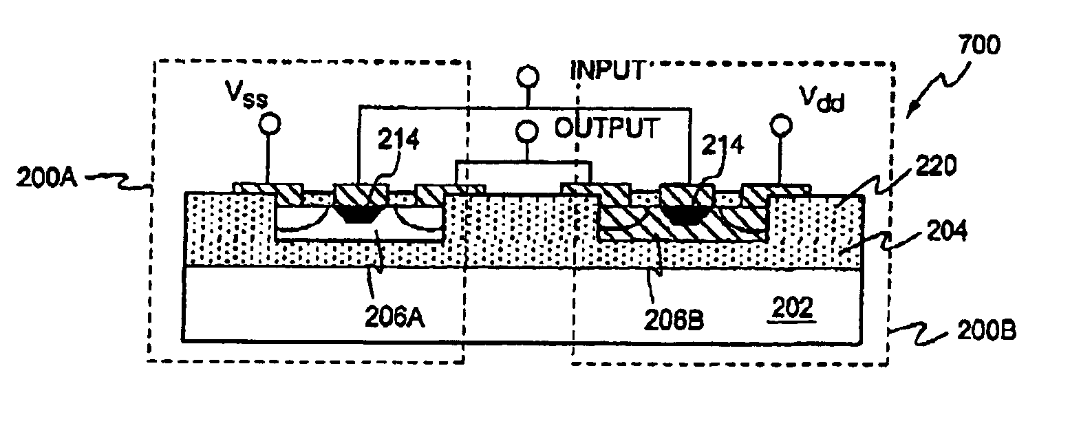
Schottky Junction Transistors (SJTs) provide numerous advantages over prior art semi-conducting devices. Several of these advantages include better transistor matching, faster switching speeds, and dramatically reduced current requirements, making the SJT particularly suitable for micro-power circuit applications. Additionally, the unique properties of the SJT allow particularly compact complementary circuits to be formed from approximately equally-sized n- and p-channel devices. Accordingly, various methods for forming semiconductor devices are provided that include the step of implanting dopants to achieve a doping concentration that allows complementary n- and p-channel SJT behavior with devices of substantially equal gate length and gate width. Moreover, complementary SJT devices are provided that include n- and p-channel devices that have approximately equal gate lengths and widths.

Problems solved by technology

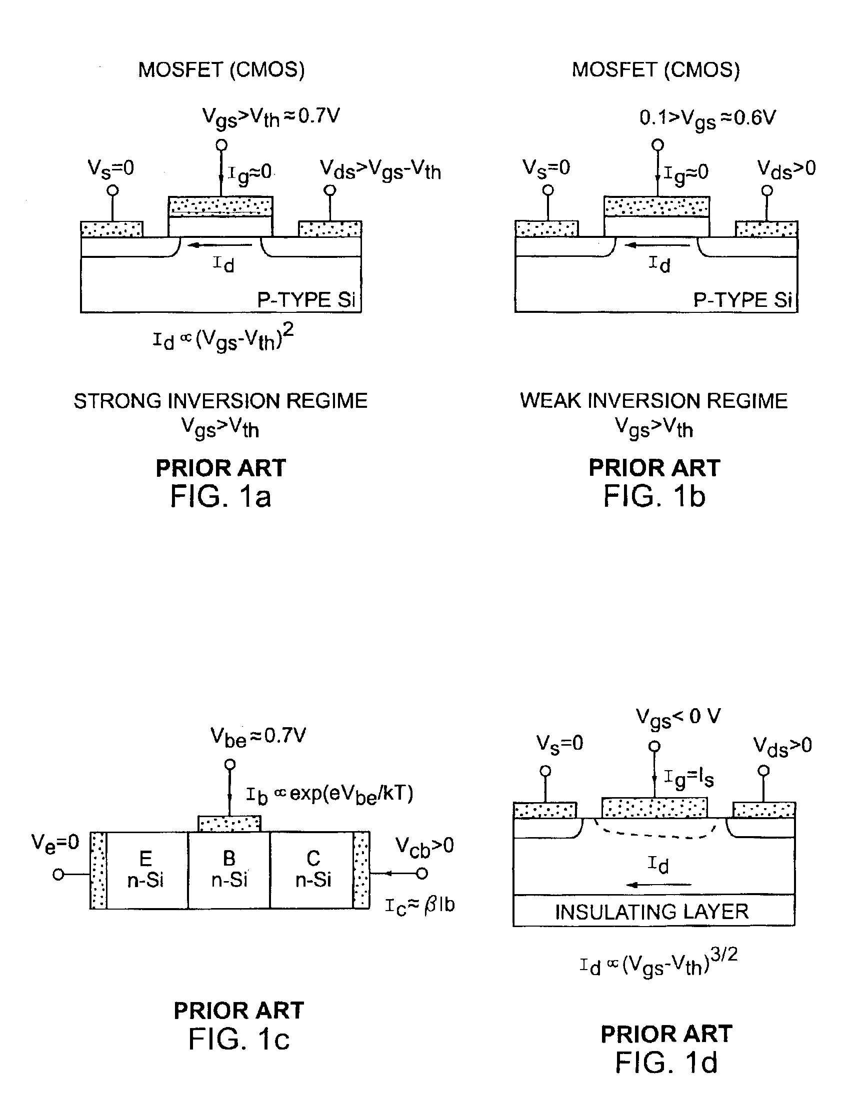
In medical devices (such as pacemakers), satellite devices, and other applications, battery replacement can be extremely inconvenient, so the need for so-called “micropower” components is increased.
The main disadvantage of such devices, however, is low speed.
Attempting to improve the speed fT of micropower devices by reducing gate length Lg, then, is not typically practical because of difficulties in precisely matching threshold voltages Vth between devices.
For this reason many micropower circuits typically have undesirably long gates (e.g. Lg≧1 μm) and typically operate below 1 MHz.
It is generally impractical to use base-emitter voltage, Vbe, to control Ic due to the exponential dependency of current (Ic) on base-emitter voltage (Vbe).
However, because BJTs are generally minority carrier devices, charging the input diffusion capacitance (i.e. Cdiff of the forward biased base-emitter junction) takes an undesirable amount of time, thus causing the cut-off frequency to be undesirably small.
BJTs therefore are typically not used as micropower devices at high frequencies.
This level of current is generally highly undesirable for micropower applications because of the associated high power consumption.
This gate leakage current is expected to limit the minimum allowable gate insulator thickness, which in turn will limit the minimum gate length of the MOSFET.

Method used


Image

  • Complementary Schottky junction transistors and methods of forming the same
  • Complementary Schottky junction transistors and methods of forming the same
  • Complementary Schottky junction transistors and methods of forming the same

Examples


Embodiment Construction

The following detailed description is merely exemplary in nature and is not intended to limit the invention or the application and uses of the invention. Furthermore, there is no intention to be bound by any expressed or implied theory presented in the preceding technical field, background, brief summary or the following detailed description.

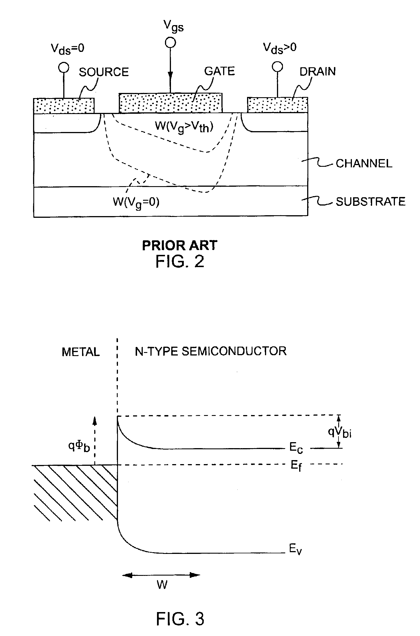
According to various aspects of the invention, an enhancement mode MESFET is produced whereby channel drain current is controlled by the application of a bias current into, or out of, the gate electrode of the MESFET. By carefully selecting channel doping, ND, channel thickness, a, and gate length, Lg, current gain greater than 1 (e.g. β>1) can be achieved for devices manufactured in accordance to the methods described below. For example, gate current control of drain current described by the present invention may be made analogous to base current control of collector current in BJTs. It is therefore appropriate that devices made in accordance w...


PUM


Abstract

Various methods for forming semiconductor devices are provided that include the step of implanting dopants into the devices to achieve doping concentrations that allow complementary n- and p-channel SJT behavior with devices of substantially equal gate length and gate width. Moreover, complementary SJT devices are provided that include n- and p-channel devices that have approximately equal gate lengths and widths. SJT devices may be appropriately doped and configured such that input current and the output current both vary substantially exponentially with a gate-source voltage in the sub-threshold mode, and such that the drain current varies substantially linearly with the gate current through a substantially constant current gain that is given by a ratio of the drain current to the gate current.

Description

TECHNICAL FIELDVarious embodiments of the present invention relate to semiconductor devices and to techniques for manufacturing semiconductor devices. More particularly, various embodiments relate to complementary field effect transistor devices that are capable of performing as current-controlled current sources.BACKGROUNDElectronic devices such as diodes, transistors and the like are commonly used in many items found in homes, offices, vehicles, personal electronics, industrial and aerospace applications, medical devices and elsewhere. Generally speaking, a transistor is a three-terminal device that provides, for example, amplification or switching capabilities in analog and digital circuits. Recently, efforts have been focused upon creating transistors that perform various functions with reduced power consumption. Reduced power consumption is particularly desirable in applications that require batteries that may need to be replaced when power is expended. In medical devices (such...

Claims


Application Information

Patent Timeline
IPC IPC(8): H01L29/66H01L29/739H01L27/085H01L29/812H01L27/095H01L29/76
CPCH01L27/095H01L29/812H01L29/7606H01L29/739
Inventor THORNTON, TREVOR J.
Owner ARIZONA STATE UNIVERSITY
Learn More