Formation of silicon-germanium-on-insulator (SGOI) by an integral high temperature SIMOX-Ge interdiffusion anneal
a technology of silicon-germanium-on-insulator and interdiffusion anneal, which is applied in the direction of water-setting substance layered product, transportation and packaging, chemistry apparatus and processes, etc., can solve the problem of high-quality buried oxide layer formation
- Summary
- Abstract
- Description
- Claims
- Application Information
AI Technical Summary
Benefits of technology
Problems solved by technology
Method used
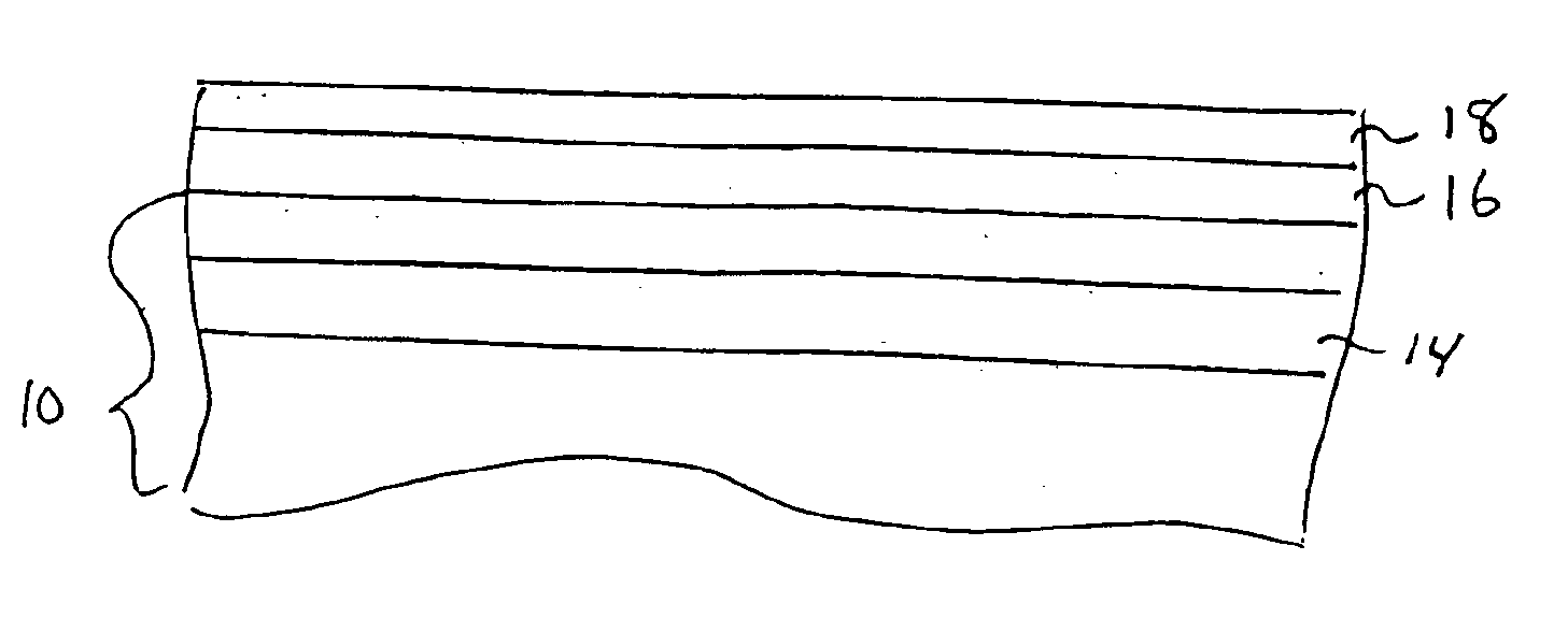
Image


Examples
example
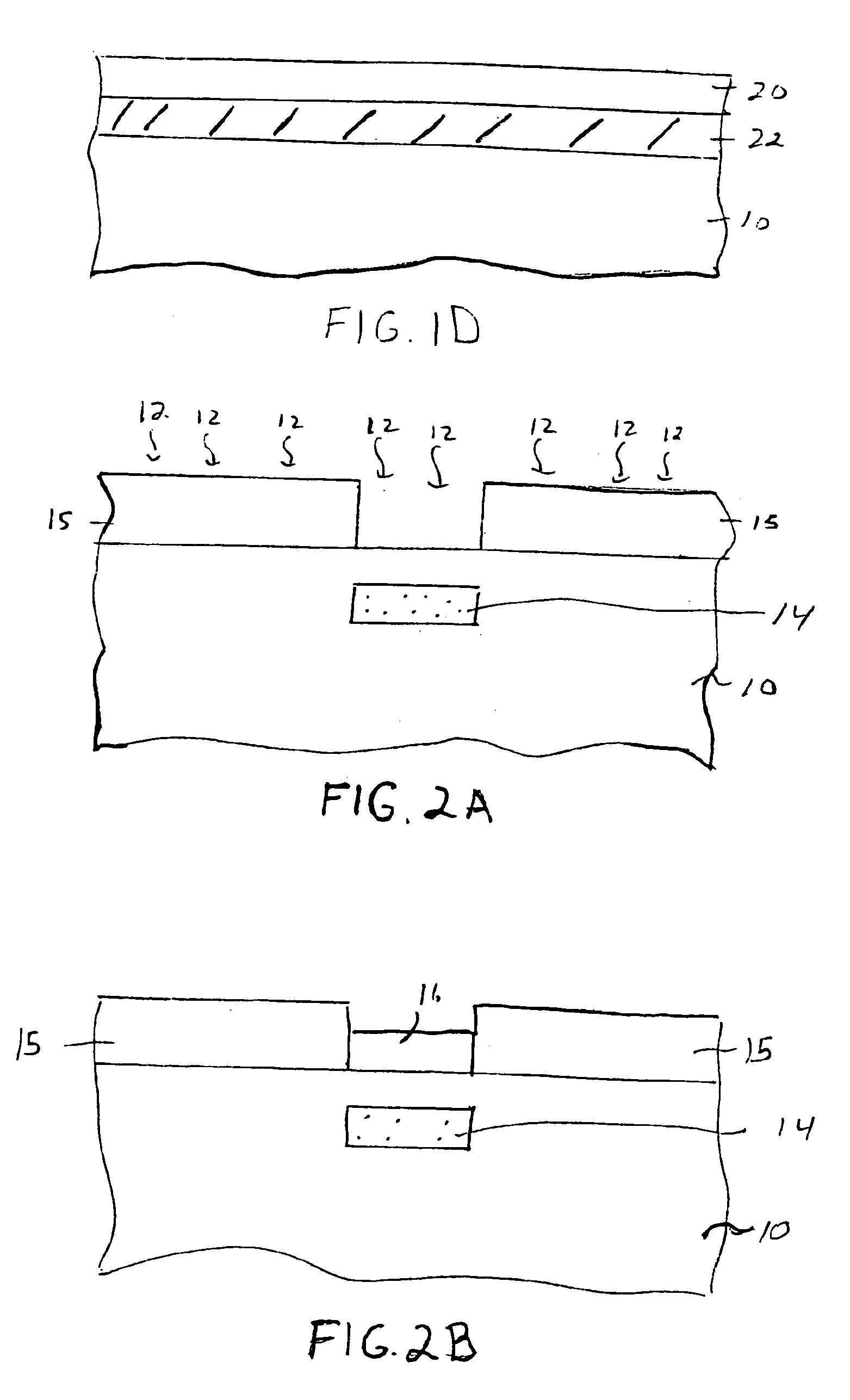
In this example, SiGe-on-insulator substrate materials were fabricated using optimal conditions that fall within the ranges mentioned above. Table 1 indicates the initial samples, oxygen implant conditions (base and second implants) and the thickness and Ge content of the Ge-containing layer grown on top of the substrate prior to oxygen implanting and heating. The heating step used in this example is as follows:ramp up from 1150° C. to 1300° C. at 0.5° C. / min in 1.5% oxygen (Ar dilution);soak at 1300° C. for 2 hours;ramp up to 1325° C. at 0.1° C. / min in an ambient comprising 50.3% oxygen and 49.7% Ar;soak at 1325° C. for 6 hours;ramp down to 1200° C. at 0.5° C. / min,oxidize at 1200° C. for 3 hours in 40% oxygen; andcool down.
Following these heating steps, the following steps were also performed:(viii) Oxide removal in 10:1 (H2O:HF) plus RCA-based wafer cleaning.(ix) Chemical-mechanical polishing and post-CMP clean(x) Epitaxial growth of strained Si layer
TABLE 1Originaltop layerSGOIBO...
PUM
| Property | Measurement | Unit |
|---|---|---|
| surface roughness | aaaaa | aaaaa |
| thickness | aaaaa | aaaaa |
| thickness | aaaaa | aaaaa |
Abstract
Description
Claims
Application Information
 - R&D
- Intellectual Property
- Life Sciences
- Materials
- Tech Scout
- Unparalleled Data Quality
- Higher Quality Content
- 60% Fewer Hallucinations
Browse by: Latest US Patents, China's latest patents, Technical Efficacy Thesaurus, Application Domain, Technology Topic, Popular Technical Reports.
© 2025 PatSnap. All rights reserved.Legal|Privacy policy|Modern Slavery Act Transparency Statement|Sitemap|About US| Contact US: help@patsnap.com