
Radiation hardened semiconductor device

Inactive Publication Date: 2005-02-15
AEROFLEX COLORADO SPRINGS INC
View PDF19 Cites 2 Cited by
  • Summary
  • Abstract
  • Description
  • Claims
  • Application Information

AI Technical Summary

Benefits of technology

An object of the present invention is to produce a radiation hardened semiconductor device that can perform in an ionizing radiation environment.
The present invention has the utility of producing a radiation hardened semiconductor device that can perform in a high radiation environment. The present invention has the further utility of producing radiation hardened semiconductor devices compatible with commercial manufacturing processes. The present invention also has the utility of suppressing the operation of parasitic transistors in the bird's beak region of a field oxide in a high radiation environment.

Problems solved by technology

LOCOS results in a transition region formed at the edges of the active region known as a bird's beak which is particularly susceptible to the formation of parasitic transistors.

Method used


Image

  • Radiation hardened semiconductor device
  • Radiation hardened semiconductor device
  • Radiation hardened semiconductor device

Examples


first embodiment

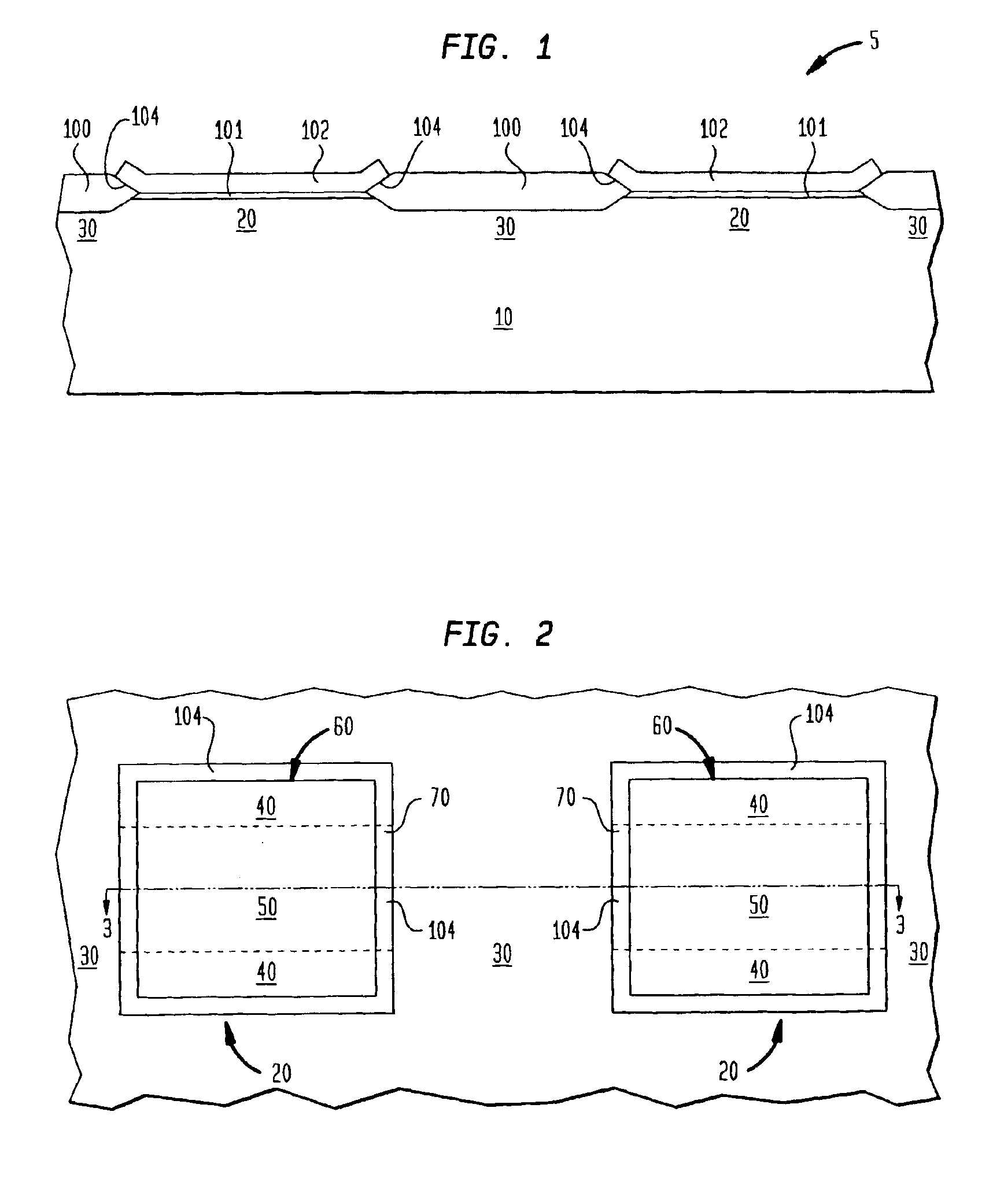
An implant barrier layer 60 is then applied to the upper surface of the field oxide 100 and the active area 20. In the preferred embodiment, the implant barrier layer 60 is photoresist, although any material that can be selectively etched relative to both silicon and silicon dioxide, and block the implant of the dopants to be implanted, may be used. FIG. 2 illustrates the pattern wherein the implant barrier layer 60 remains over the active area 20 while exposing the implant area 70. The implant area 70 is defined as the active portion of area 20 that comprises the bird's beak region 104 of the field oxide 100. The isolation region 30 is also exposed.

An implant of the implant area 70 and the isolation region 30 is performed using a P-type dopant such as boron. In the preferred embodiment the boron is implanted at a dose within a range of 1×10¹¹ ion / cm2 to 5×10¹⁴ ions / cm2 at an energy level within a range 20 keV to 100 keV at an implant angle of 0 to 45° with a preferred angle of 0°....

second embodiment

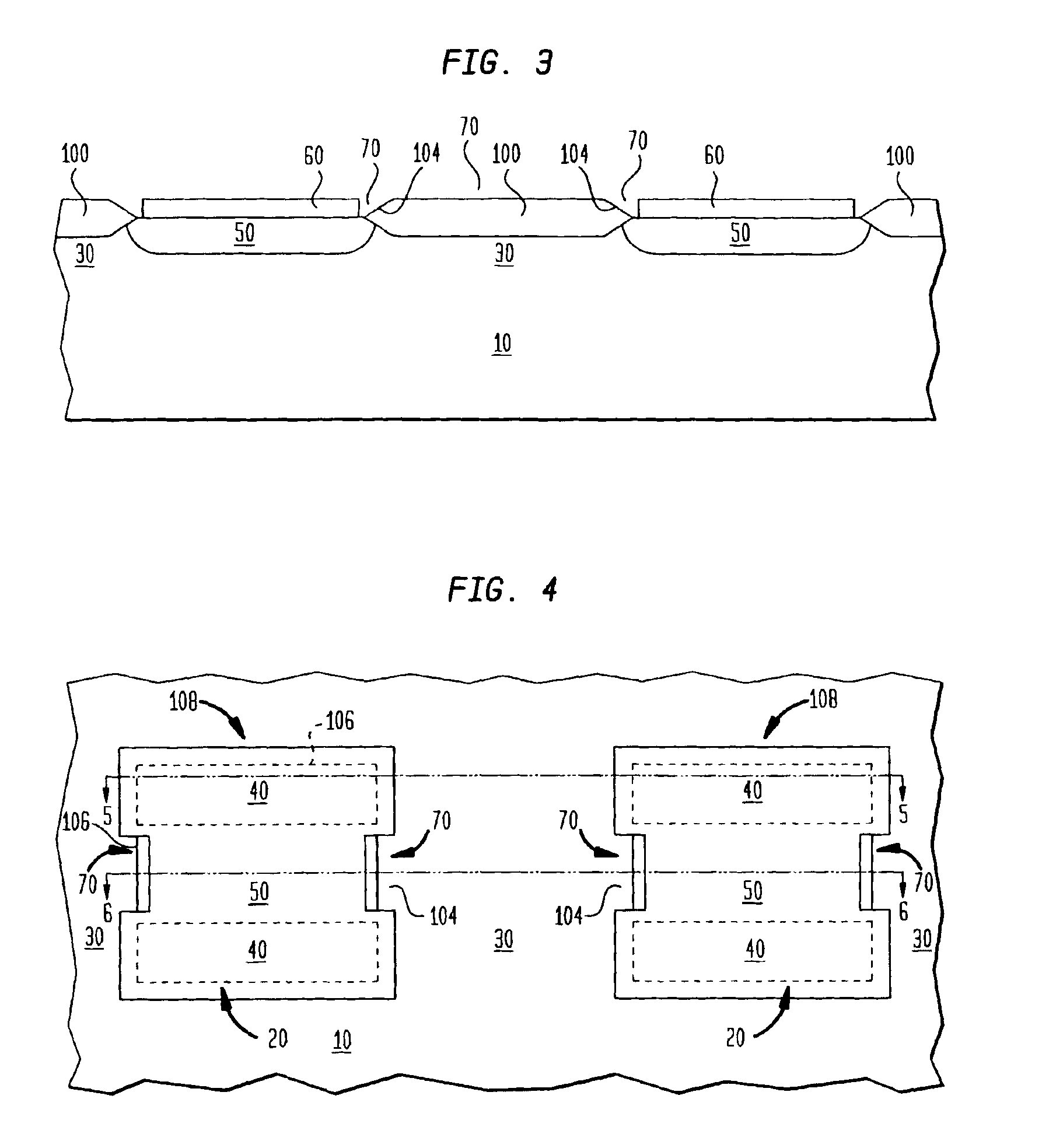
In the subject invention, the process follows the same steps as the preferred embodiment with the exception that an implant barrier 60 is applied prior to the first implant. The cross section of the implant barrier 60 is shown in FIG 3. The implant barrier 60 is removed prior to annealing the first implant.

third embodiment

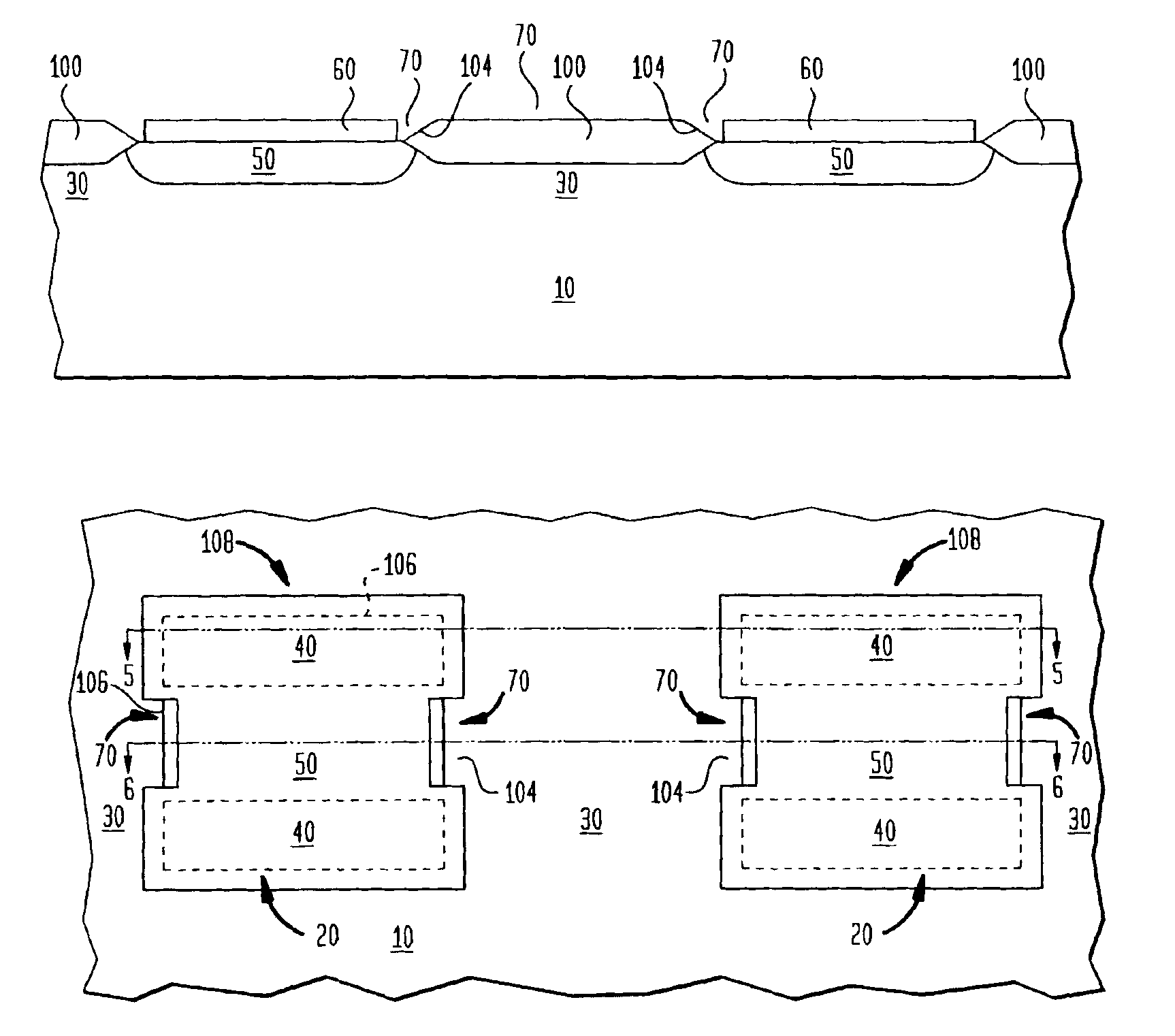
A third and fourth embodiment of the subject invention are illustrated in FIGS. 4 through 6. The process for the third embodiment follows the same steps as the preferred embodiment with the exception that the implant barrier 108 is defined to expose a portion of the active area 20 that comprises the bird's beak region 104 that will subsequently underlie the gate layer.

The process of the fourth embodiment follows the same steps of second embodiment with the exception that the implant barrier 108 is defined to expose a portion of the active area 20 that comprises the bird's beak region 104 that will subsequently underlie the gate layer.


PUM


Abstract

A method for manufacturing a radiation hardened semiconductor device, having defined active region and isolation region. The isolation region containing an isolation material and active region containing a transition region between active and isolation region, sometimes denoted a bird's beak region. Wherein the transition region is implanted with germanium and boron, to prevent formation of leakage paths between active devices, or within an active device. The implanted area can be further limited to that area of the transition region that is adapted to be covered by a gate material, such as polysilicon.

Description

TECHNICAL FIELDThis invention relates to radiation hardening of semiconductor devices and more particularly to radiation hardening of the birds beak region to prevent formation of leakage paths in high radiation environments.BACKGROUND ARTThe field of radiation hardening in semiconductor devices deals in part with the problem of electron-hole pairs generated by the passage of ionizing radiation through the semiconductor devices. Electron-hole pairs generated in the bulk silicon do not present a severe problem, as the electrons and holes recombine rapidly. Electron-hole pairs formed in silicon dioxide are more difficult to deal with because the electrons are far more mobile than the holes and may become separated from the holes, making recombination more difficult and resulting in an accumulation of net positive charge in the silicon dioxide, or other dielectric film.The conventional process for laterally isolating semiconductor circuits uses a field oxide between the active regions....

Claims


Application Information

Patent Timeline
IPC IPC(8): H01L21/70H01L21/265H01L21/02H01L21/762
CPCH01L21/76202H01L21/26506H01L21/2658
Inventor WOODRUFF, RICHARD L.TYSON, SCOTT M.CHAFFEE, JOHN T.KERWIN, DAVID B.
Owner AEROFLEX COLORADO SPRINGS INC
Learn More