Ferroelectric memory and method of reading data in the same
a technology of ferroelectric memory and data, applied in the field of ferroelectric memory, can solve the problems of reduced read margin, deterioration of data write characteristic of ferroelectric capacitor, and loss of written data, and achieve the effects of reducing the influence of depolarization, low cost, and adding security functions to ferroelectric memory with eas
- Summary
- Abstract
- Description
- Claims
- Application Information
AI Technical Summary
Benefits of technology
Problems solved by technology
Method used
Image
Examples
first embodiment
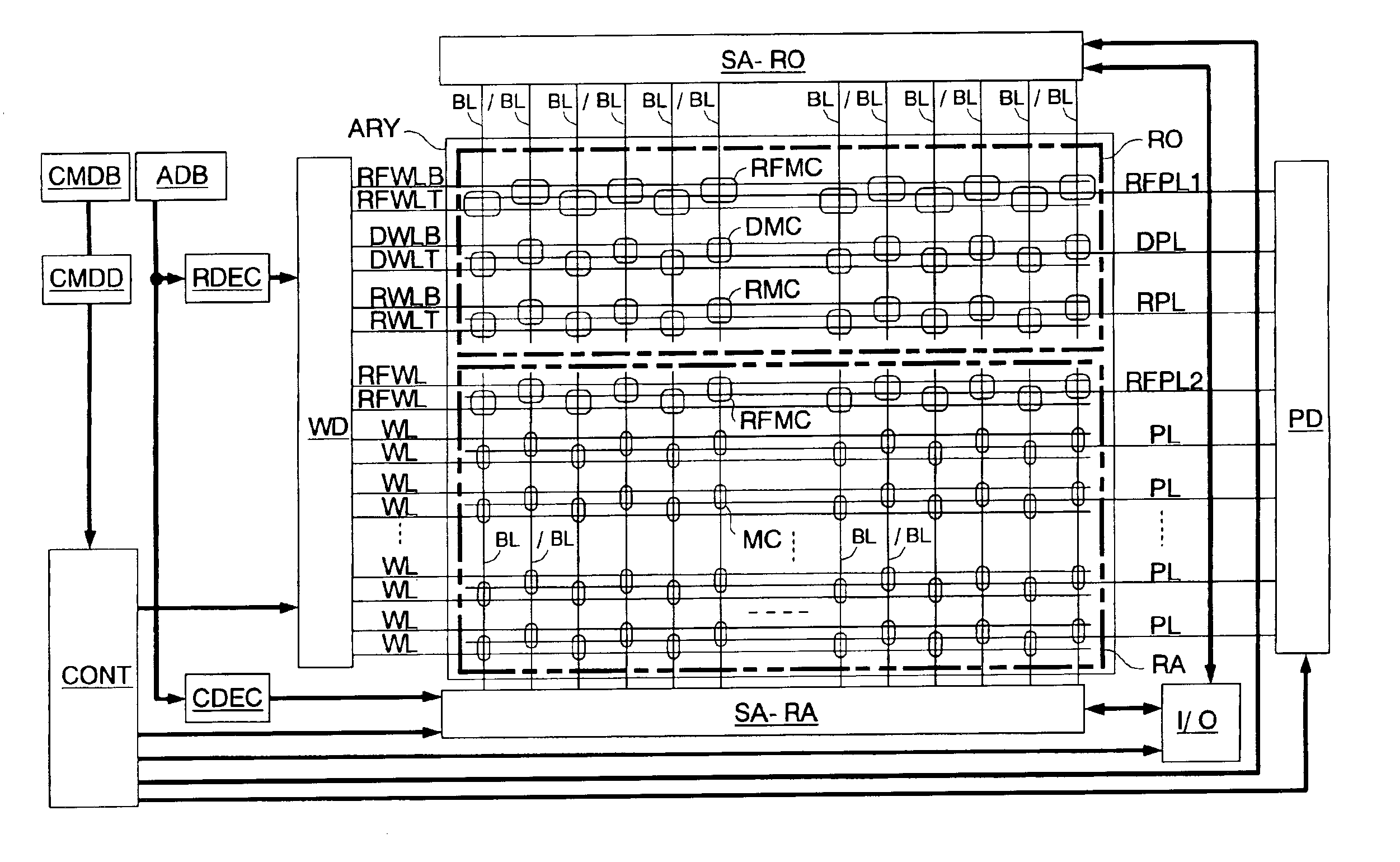
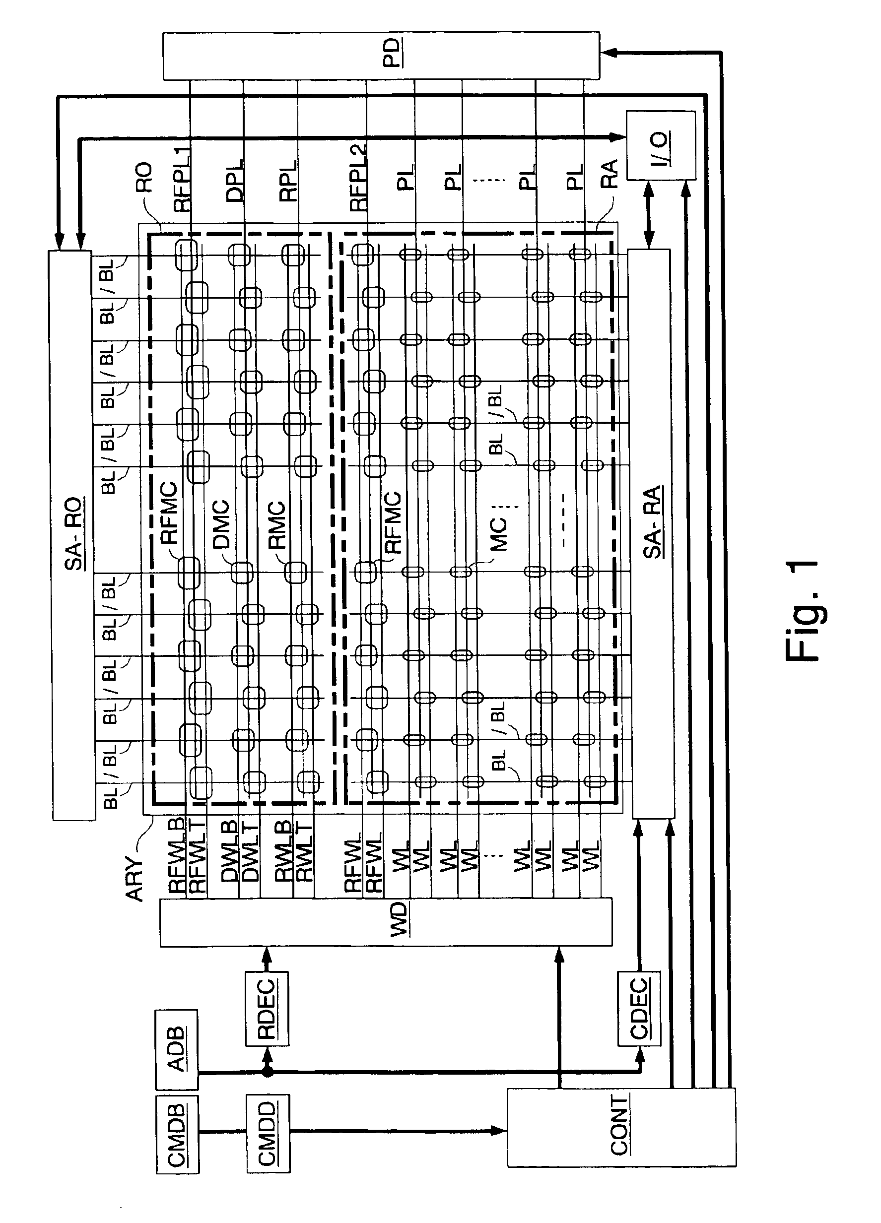
FIG. 1 shows a ferroelectric memory and a method of reading data in the ferroelectric memory according to the present invention.
The ferroelectric memory is formed on a silicon substrate with the use of CMOS process. The ferroelectric memory mounted on, for example, an IC card is used as a security chip. To use the ferroelectric memory as the security chip, authentication data is written thereinto in a test process of manufacturing process. Pads formed in the ferroelectric memory chip are soldered to the printed-wiring board of the IC card and the like, so that the ferroelectric memory chip is mounted on the IC card. Soldering is carried out with, for example, infrared reflow.
The ferroelectric memory has a command buffer CMDB, a command decoder CMDD, an address buffer ADB, a control circuit CONT, a row decoder RDEC, a column decoder CDEC, a word driver row WD, a memory cell array ARY, sense amplifier rows SA-RO and SA-RA, a plate driver row PD, and a data input / output circuit I / O.
The...
second embodiment
In this embodiment, the plate lines PLs are wired orthogonally to the word lines RFWLB, RFWLT, DWLB, DWLT, RWLB, RWLT, and WLs. In other words, the ferroelectric memory according to the present invention adopts a word line / plate line cross technique. In the word line / plate line cross technique, it is possible to select only the plate line / lines connected to the memory cell / cells actually carrying out the read operation, in accordance with the selection of the word line. Thus, since the operation of drivers unnecessary for memory operation stops in the plate driver row PD, power consumption can be reduced. The plate driver row PD is opposed to the sense amplifier row SA-RA across the memory cell array ARY. The rest of the structure is almost the same as that of the
FIG. 11 shows the details of essential portions of the ROM area RO shown in FIG. 10.
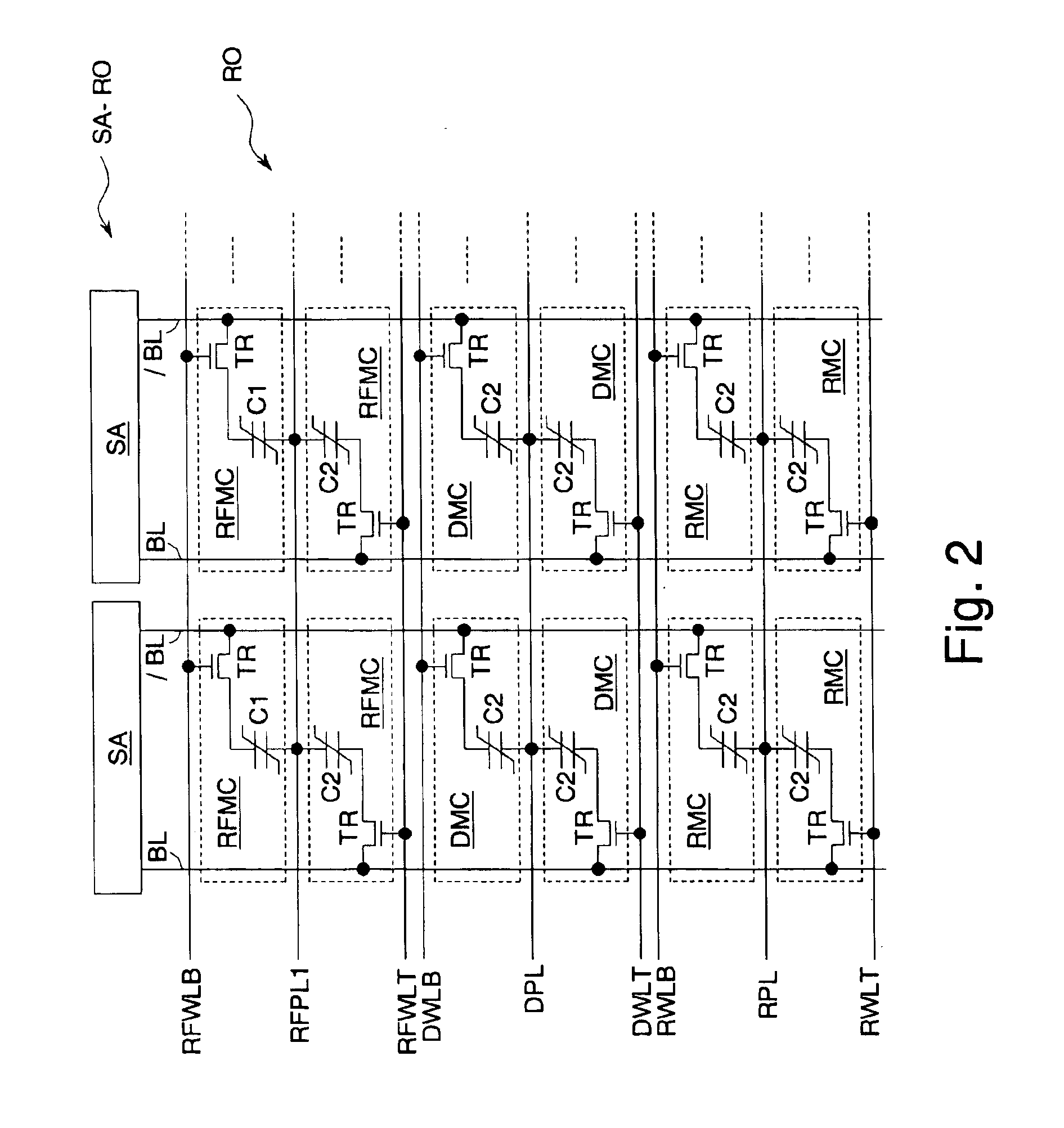
The ROM area RO is almost identical to that of FIG. 2, except that the plate lines PLs are wired orthogonally to the word lines RFWLB, RFWL...
PUM
 Abstract
Description
Claims
Application Information
 - R&D
- Intellectual Property
- Life Sciences
- Materials
- Tech Scout
- Unparalleled Data Quality
- Higher Quality Content
- 60% Fewer Hallucinations
Browse by: Latest US Patents, China's latest patents, Technical Efficacy Thesaurus, Application Domain, Technology Topic, Popular Technical Reports.
© 2025 PatSnap. All rights reserved.Legal|Privacy policy|Modern Slavery Act Transparency Statement|Sitemap|About US| Contact US: help@patsnap.com


