
Semiconductor memory device and production method of the same

a memory device and semiconductor technology, applied in the direction of semiconductor devices, semiconductor/solid-state device details, capacitors, etc., can solve the problems of long write time, affecting high-speed operation, and presenting a considerable problem

Inactive Publication Date: 2001-11-06
SHARP KK
View PDF6 Cites 54 Cited by
  • Summary
  • Abstract
  • Description
  • Claims
  • Application Information

AI Technical Summary

Benefits of technology

Thus, the invention described herein makes possible the advantages of (1) providing a semiconductor memory device incorporating a ferroelectric capacitor which exhibits excellent ferroelectric characteristics, and (2) providing a method for producing such a semiconductor memory device with high yield.

Problems solved by technology

However, they require a long write time, thereby hindering high-speed operation.
This presents a considerable problem.
The aforementioned movement of oxide through the Pt film presents another problem in that, in the case where a closely contacting film is employed in a Pt / Ta / TiN / Ti structure or a Pt / Ti / TiN / Ti structure, an insulating material may be formed as a result of oxidation of the Ta or Ti immediately underlying the Pt, thereby disrupting the electrical connection.
Thus, constructing an electrode only from a Pt film, or a combination of a Pt film and a closely contacting film can result in marked problems associated with hillocks and / or insufficient electrical contact due to the oxidation of a diffusion barrier film such as TiN.
These problems make it difficult to realize stacked type structures.
However, again such a structure is susceptible to the problem of insufficient electrical contact due to oxidation of the polysilicon at the IrO.sub.2 / polysilicon interface, as well as silicidation of IrO.sub.2 formed immediately above the polysilicon, during the IrO.sub.2 film formation and the ferroelectric film formation.
In the Pt / TiN / Ti structure, an insulating material may be formed at such a high temperature as a result of oxidation of the Ti which is a closely contacting film, thereby disrupting the electrical conduction.
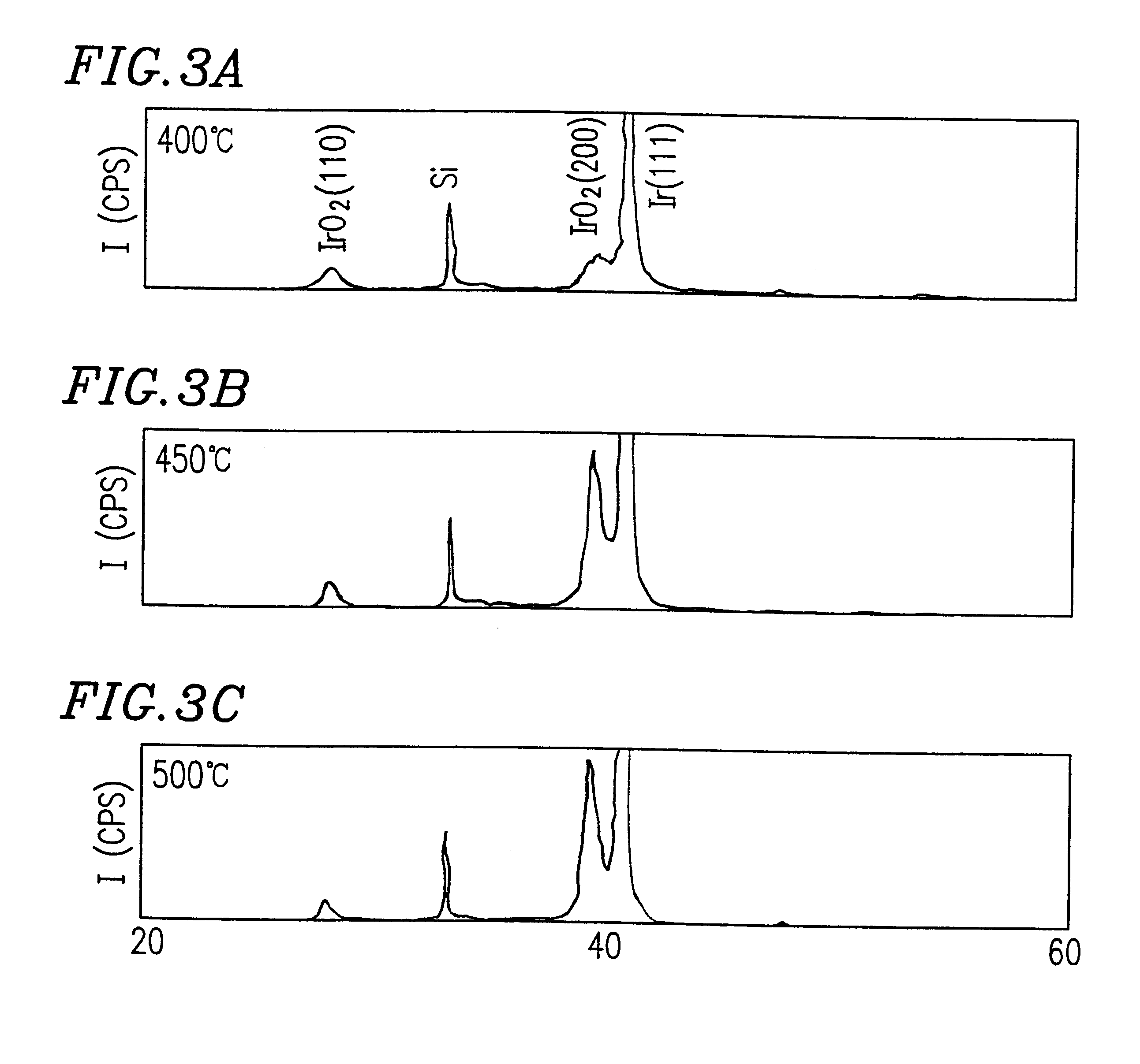
However, when the IrO.sub.2 film is formed directly on the Ir film at a high temperature, the IrO.sub.2 film becomes non-uniform in quality, making it impossible to form a homogenous film at a high temperature.
Moreover, hillocks or the like may be produced in a high-temperature atmosphere due to the poor anti-heat properties of the diffusion barrier film.
However, in the stacked type structure which is essential to achieve a high-density integration of the ferroelectric memories, a polysilicon plug typically used to establish contact with a lower electrode and / or a diffusion barrier layer (barrier metal layer), e.g., TiN or TaSiN, for preventing diffusion between the plug and the lower platinum electrode, tend to be oxidized during the high-temperature process.
Such oxidation of the polysilicon plug and / or diffusion barrier layer (barrier metal layer), if it occurs, may disrupt electrical conduction between the plug and the lower electrode, and / or may cause peeling due to expansion of the barrier metal.

Method used


Image

  • Semiconductor memory device and production method of the same
  • Semiconductor memory device and production method of the same
  • Semiconductor memory device and production method of the same

Examples


example 2

(Example 2)

A process of producing a ferroelectric memory device according to Example 2 of the present invention will now be described with reference to FIGS. 7 and 8A to 8D.

First, a thermal oxide film (SiO.sub.2 film) 202 having a thickness of about 200 nm is formed on a silicon substrate 201 by heat-treatment in an oxygen atmosphere containing vapor at about 1050.degree. C. for about 20 minutes. Then, a Ti film having a thickness of about 20 nm is formed on the thermal oxide film 202 by sputtering Ti at a DC power of about 2 kW and a substrate temperature of about 400.degree. C. A closely contacting TiO.sub.2 film 203 having a thickness of about 40 nm is formed by thermally oxidizing the Ti film. Thereafter, a lower Pt electrode 204 having a thickness of about 200 nm is formed by sputtering Pt at a DC power of about 2 kW and a substrate Ad temperature of about 500.degree. C. Thus, a Pt / TiO.sub.2 / SiO.sub.2 / Si substrate as shown in FIG. 8A is prepared.

Then, an MOD solution of ferro...

example 3

(Example 3)

A process of producing a ferroelectric memory device according to Example 3 of the present invention will now be described with reference to FIGS. 11 and 12A to 12C.

First, a thermal oxide film (SiO.sub.2 film) 302 having a thickness of about 200 nm is formed on a silicon substrate 301 by heat-treatment in an oxygen atmosphere containing vapor at about 1050.degree. C. for about 20 minutes. Then, a Ti film having a thickness of about 20 nm is formed on the thermal oxide film 302 by sputtering Ti at a DC power of about 2 kW and a substrate temperature of about 400.degree. C. A closely contacting TiO.sub.2 film 303 having a thickness of about 40 nm is formed by thermally oxidizing the Ti film. Thereafter, a lower Pt electrode 304 having a thickness of about 200 nm is formed by sputtering Pt at a DC power of about 2 kW and a substrate temperature of about 500.degree. C. Thus, a Pt / TiO.sub.2 / SiO.sub.2 / Si substrate as shown in FIG. 12A is prepared.

Then, an MOD solution of ferr...

example 4

(Example 4)

A process of producing a ferroelectric memory device according to Example 4 of the present invention will now be described with reference to FIGS. 16 and 17A to 17D.

First, a Pt / TiO.sub.2 / SiO.sub.2 / Si substrate including a silicon substrate 401, a thermal oxide film (SiO.sub.2 film) 402 having a thickness of about 200 nm, a closely contacting TiO.sub.2 film 403 having a thickness of about 40 nm, and a lower Pt electrode 404 having a thickness of about 200 nm is prepared by the same process as in Example 2 (see FIG. 17A).

Then, an MOD solution of ferroelectric material SrBi.sub.2 Ta.sub.2 O.sub.9 (Sr / Bi / Ta=8 / 24 / 20) produced as in the case of Example 1 is applied on the Pt / TiO.sub.2 / SiO.sub.2 / Si substrate by a spin-coating method at a rotational speed of about 3000 rpm so that each layer has a thickness of about 50 nm (Step 451). The resultant substrate is dried in air at 250.degree. C. for about 5 minutes (Step 452). Thereafter, the substrate is pre-baked in a normal-pre...


PUM


Abstract

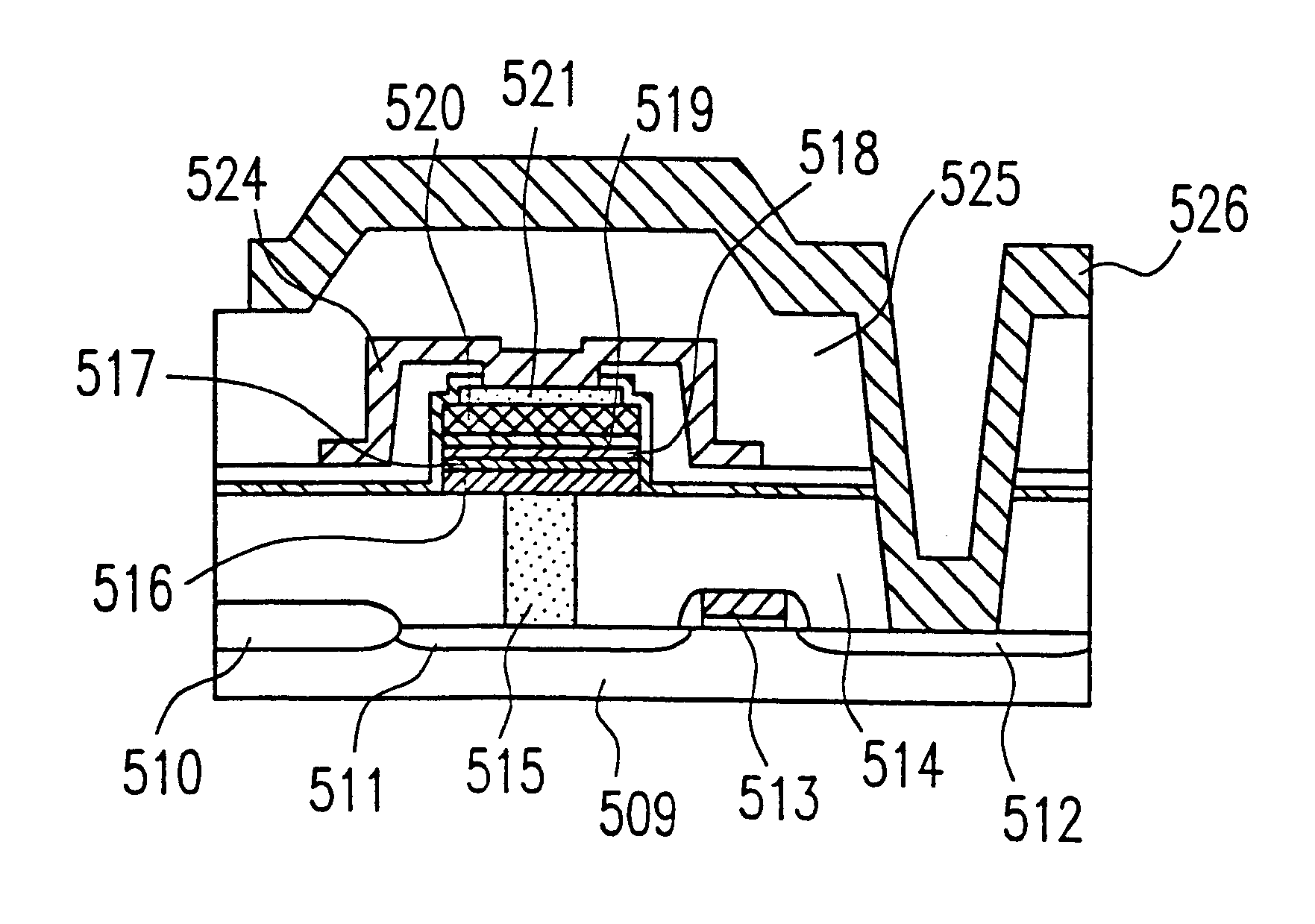
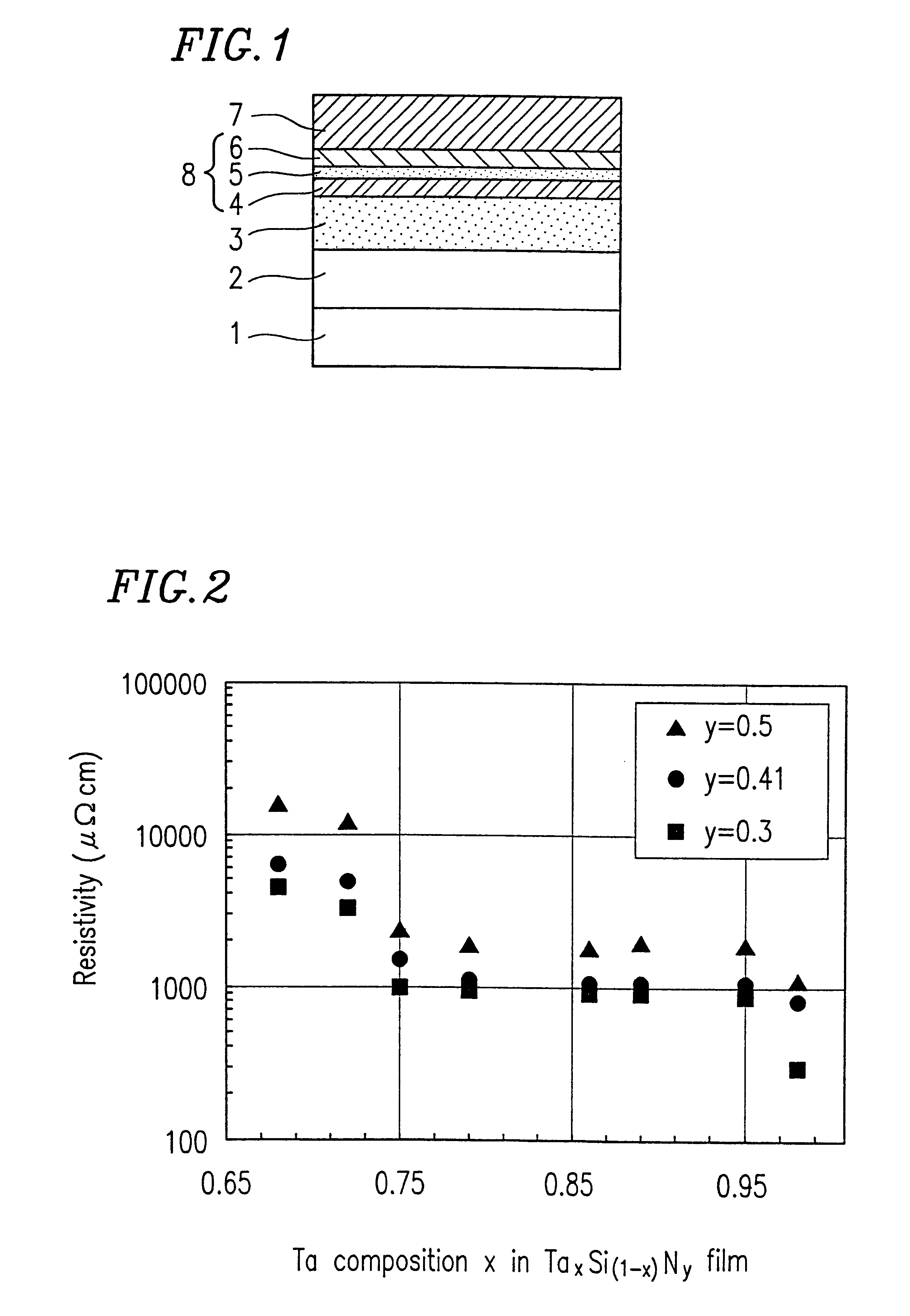
A semiconductor memory device includes: a capacitor formed on a substrate and including a lower electrode, a dielectric film and an upper electrode; a selection transistor formed at the substrate; an electrically conductive plug for providing electrical connection between the selection transistor and the capacitor; and a diffusion barrier film provided between the electrically conductive plug and the lower electrode of the capacitor. The diffusion barrier film is a TaxSi1-xNy film or a HfxSi1-xNy film (where 0.2<x<1 and 0<y<1). The lower electrode includes an Ir film and an IrO2 film which are sequentially formed.

Description

1. Field of the InventionThe present invention relates to a semiconductor memory device and a method for producing the same. In particular, the present invention relates to a semiconductor memory device incorporating a capacitor which includes a lower electrode, a dielectric film, and an upper electrode, the capacitor being electrically connected to a selection transistor via an electrically conductive plug and a diffusion barrier film, as well as a method for producing the same. The present invention further relates to a method for producing a capacitor for use in such a semiconductor memory device, the capacitor including a ferroelectric film (hereinafter, such a capacitor will also be referred to as a "ferroelectric capacitor"), as well as a method for producing a non-volatile semiconductor memory device incorporating such a ferroelectric capacitor.2. Description of the Related ArtFerroelectric materials have a large range of applications for various devices utilizing their funct...

Claims


Application Information

Patent Timeline
Patent Type & Authority Patents(United States)
IPC IPC(8): H01L21/02H01L21/70H01L27/115H01L21/768H01L21/8246H01L21/316H10B20/00H10B69/00
CPCH01L21/31683H01L21/76841H01L21/76864H01L21/7687H01L27/11502H01L27/11507H01L28/75H01L28/55H01L2924/0002H01L2924/00H01L21/0215H01L21/02148H10B53/30H10B53/00
Inventor YOKOYAMA, SEIICHIMITARAI, SHUNNAGATA, MASAYAKUDO, JUNOGATA, NOBUHITOITOH, YASUYUKI
Owner SHARP KK
Learn More