
All-optical mach-zehnder wavelength converter with monolithically integrated laser

a wavelength converter and monolithic laser technology, applied in the field of interferometer wavelength converters, can solve problems such as coupling losses

Inactive Publication Date: 2001-03-27
AVAGO TECH WIRELESS IP SINGAPORE PTE +2
View PDF3 Cites 52 Cited by
  • Summary
  • Abstract
  • Description
  • Claims
  • Application Information

AI Technical Summary

Benefits of technology

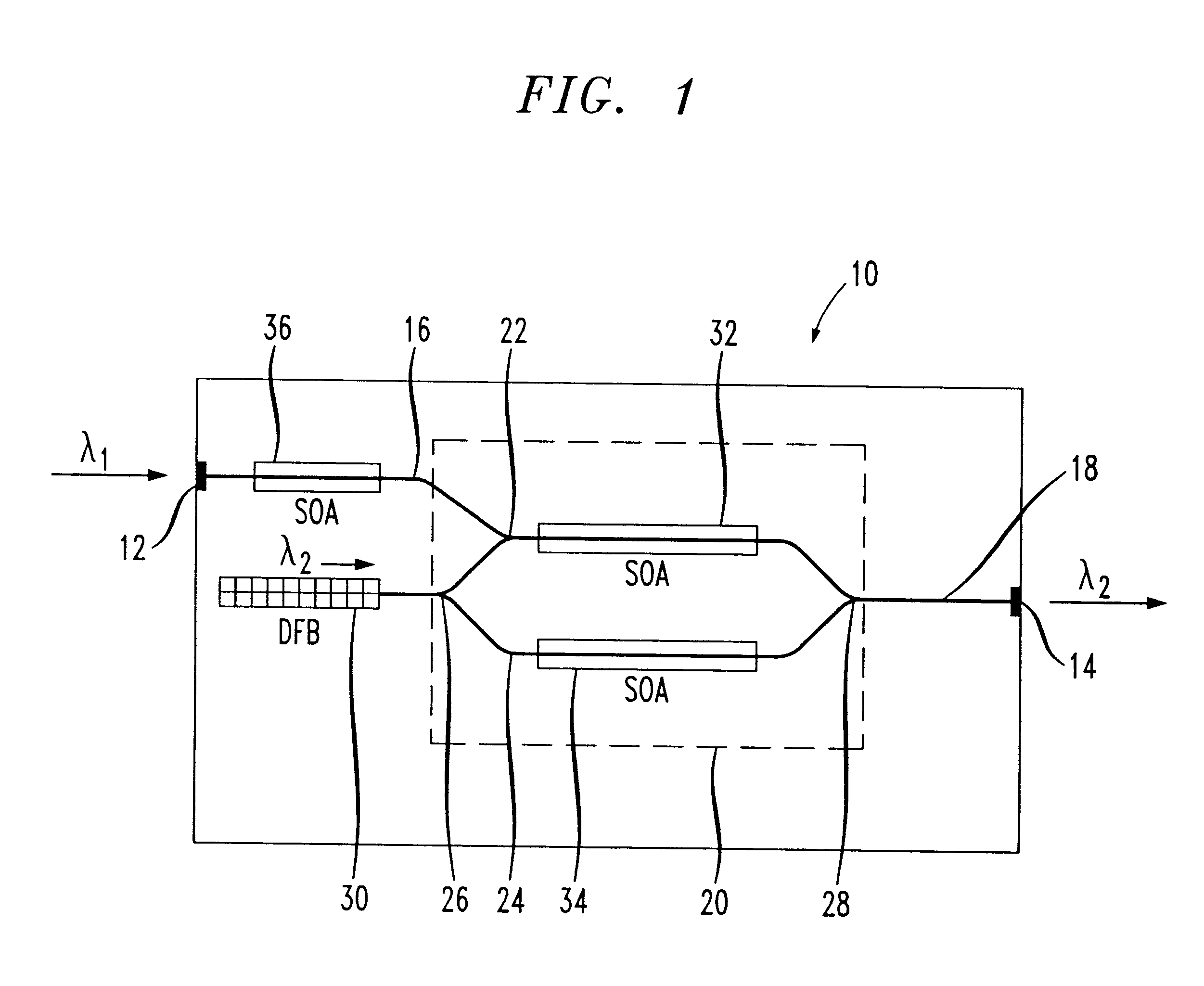
The inventive device 10 further includes an integrated on-chip optical source, such as a distributed feedback (DFB) continuous wave source or laser 30, connected to the input terminal 26 of the interferometer 20 to provide optical power at a given wavelength (.lambda..sub.2) for interferometer operation. In a preferred embodiment, laser 30 is a 1 / 4-wave shifted DFB laser. The optical power signal generated by laser 30 is divided between the first and second branches 22, 24 of the interferometer, as is known in the art. By applying the input signal .lambda..sub.1 to one of the branches (e.g. the first branch 22), stimulated emission caused by input signal .lambda..sub.1 reduces the carrier density within the semiconductor optical amplifier (e.g. 32), which causes a change in the optical path length of that branch, resulting in a change in the output power of the signal .lambda..sub.2 at the output 28 of the interferometer 20.
As is known by those having ordinary skill in the art, Mach-Zehnder interferometers require a .pi. phase difference between their arms for complete switching. This .pi. phase shift is achieved for a particular input power level of the signal at .lambda..sub.1 at port 16, which depends on the operating and manufacturing details of the interferometer 20 and input waveguide 16. In the three-port prior art wavelength conversion device discussed above, the operation of the Mach-Zehnder interferometer 20 is therefore susceptible to variations in the power of the input signal .lambda..sub.1. Thus, as the input signal power varies, the Mach-Zehnder interferometer requires continuous adjustment for proper system operation, as for example by adjusting the electrical bias current to semiconductor optical amplifiers 32 or 34, to compensate for variation in the input data signal power. In order to compensate for variations in input signal power a semiconductor optical amplifier 36 is preferably provided on input waveguide 16 between input port 12 and first branch 22. The semiconductor optical amplifier 36 enables dynamic adjustment of the power of the input signal .lambda..sub.1 to the appropriate operating range of the Mach-Zehnder interferometer 20 by variation of its electrical bias current. It has been discovered that by incorporating the semiconductor optical amplifier 36 at the input port 12, the Mach-Zehnder operating range can be advantageously extended to accommodate lower power levels.
The device 10 may be fabricated using well-known fabrication techniques, such as photonic integration processes from a standard MOVPE-grown wafer containing multiple quantum-well active layers formed on a passive InGaAsP waveguide core, as has been used to fabricate test devices. The quantum wells consist of an optimized compressively / tensile strained stack to provide polarization independent gain. The gratings in the DFB laser 30 are preferably formed by phasemask printing, thus enabling the fabrication of devices emitting many different wavelengths on a single wafer. The quantum wells are etched away in the passive sections before waveguide formation.

Problems solved by technology

However, it suffers from coupling losses resulting from coupling the continuous wave input to the interferometer, and from polarization variations of the continuous wave input.

Method used


Image

  • All-optical mach-zehnder wavelength converter with monolithically integrated laser
  • All-optical mach-zehnder wavelength converter with monolithically integrated laser
  • All-optical mach-zehnder wavelength converter with monolithically integrated laser

Examples


Embodiment Construction

With reference to FIG. 1, a wavelength converter device 10 having an integrated (on-chip) laser in accordance with the present invention is there depicted. As shown, the device contains an input port 12 for receiving an optical data signal .lambda..sub.1, and an output port 14 for outputting a signal .lambda..sub.2. Output signal .lambda..sub.2 contains the data information of input signal .lambda..sub.1 and is shifted or converted to a different wavelength (e.g. .lambda..sub.2) by the device 10. An on-chip interferometer 20, such as a Mach-Zehnder interferometer, is connected between the input port 12 and the output port 14 via an input waveguide 16 that provides input signal .lambda..sub.1 to the interferometer, and an output waveguide 18 that carries .lambda..sub.2 to output port 14.

As shown in FIG. 1, interferometer 20 has a first branch 22 and a second branch 24 having a common input terminal 26 and a common output terminal 28, with each branch containing a respective semicondu...


PUM

PropertyMeasurementUnit
lengthaaaaaaaaaa
conversion gainaaaaaaaaaa
wavelengthsaaaaaaaaaa

Abstract

A wavelength converter incorporating an on-chip integrated laser for use in an optical system. The converter includes a first port for receiving an optical input signal such as a WDM signal and providing it to an interferometer, and an output port for outputting a signal which is a wavelength-converted version of the input signal. An optical source or laser is fabricated on the chip substrate on which the interferometer is formed for providing operating power to the interferometer. Power levels of the input signal are maintained by adjusting an on-chip semiconductor optical amplifier that receives the optical input signal and provides the amplified signal to the interferometer. In an alternative embodiment, the on-chip optical source is replaced by an on-chip pre-amplifier for an external laser source.

Description

I. Field of the InventionThe present invention relates to a wavelength converter for use in wavelength division multiplexed optical communications systems. More particularly, the present invention is directed to an interferometer wavelength converter having an integrated continuous wave probe source and / or integrated optical pre-amplifier(s).II. Description of the Related ArtWavelength division multiplex (WDM) networks benefit from the flexibility of wavelength converters due to the reduction in network blocking probability that such converters provide and because wavelength conversion at selected nodes in the network enables decentralized wavelength allocation management. One of the most-practical all-optical wavelength conversion schemes is cross-phase modulation in an interferometric configuration containing semiconductor optical amplifiers (SOA). Essentially, such a configuration consists of a three-port interferometer device, such as a Michelson or Mach-Zehnder interferometer, ...

Claims


Application Information

Patent Timeline
Patent Type & Authority Patents(United States)
IPC IPC(8): G02F2/00H01S5/50H01S5/026H01S5/00G02F1/01G02F1/21H01S5/12
CPCG02F2/004H01S5/026H01S5/50G02F2001/212H01S5/12G02F1/212
Inventor KOREN, UZIELSPIEKMAN, LEONARD HENRIWIESENFELD, JAY M.
Owner AVAGO TECH WIRELESS IP SINGAPORE PTE
Learn More