Semiconductor device and manufacturing method thereof for removing reaction products of dry etching
a semiconductor device and reaction product technology, applied in the direction of electrical appliances, decorative surface effects, decorative arts, etc., can solve the problems of large number of steps, long processing time, and failure to disclose any technique for removing reaction products of dry etching and resist masks
- Summary
- Abstract
- Description
- Claims
- Application Information
AI Technical Summary
Problems solved by technology
Method used
Image

Examples
first embodiment
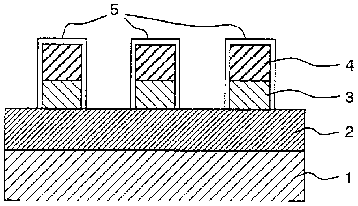
FIGS. 1A, 1B, and 1C are process diagrams for description of a manufacturing method of a semiconductor device according to a first embodiment of the present invention. In the first embodiment, a liquid chemical is selected so that only reaction products of dry etching are removed while a resist mask is left.
FIGS. 1A, 1B, and 1C are schematic sectional views showing states before the start of first dry etching, after the end of the first dry etching, and after the end of first wet etching, respectively.
First, as shown in FIG. 1A, a silicon oxide (SiO.sub.2) film 2 of, for instance, 1,000 nm in thickness is formed on the surface of a silicon substrate 1 by thermal oxidation. A 300-nm-thick polysilicon film 3 as, for instance, a wiring electrode material is deposited on the silicon oxide film 2 by chemical vapor deposition (CVD). Further, a photoresist of about 1,000 nm in thickness is applied to the polysilicon film 3 by spin coating, and then patterned into a resist mask 4 as an etch...
second embodiment
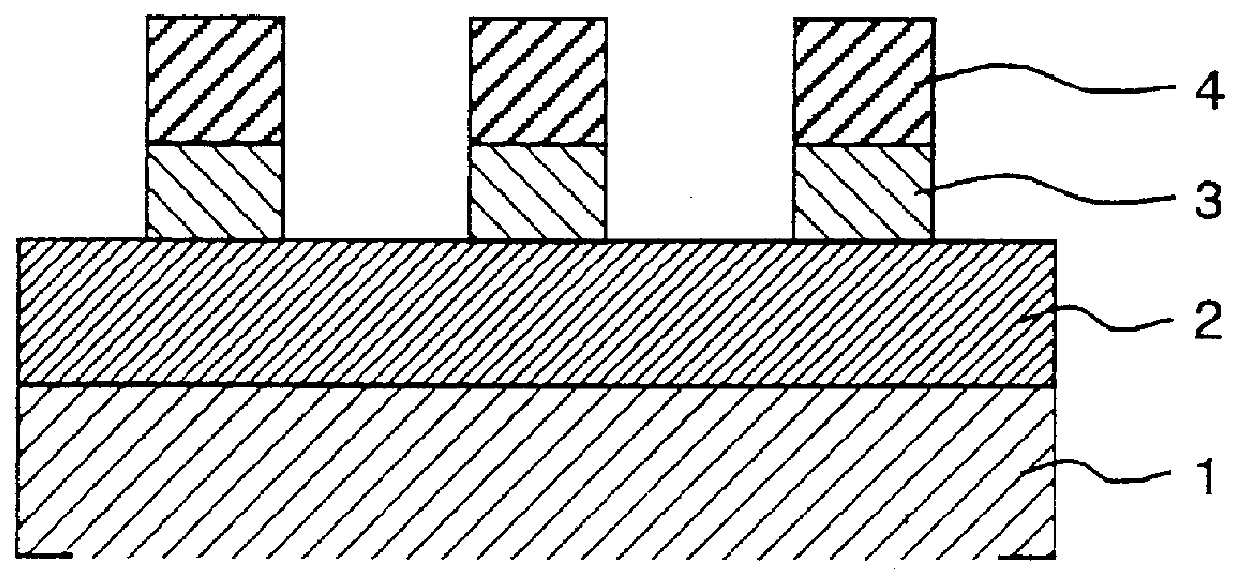
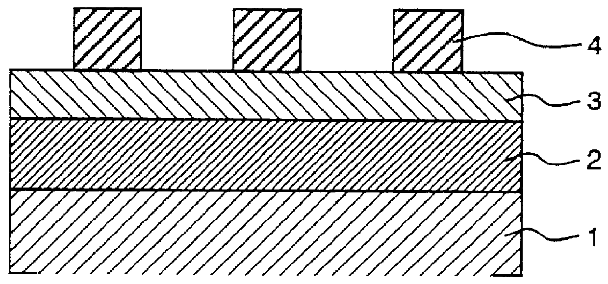
FIGS. 2A, 2B, and 2C are process diagrams for description of a manufacturing method of a semiconductor device according to a second embodiment of the invention. In the second embodiment, a liquid chemical is selected so that a resist mask is removed together with dry etching reaction products.
FIGS. 2A, 2B, and 2C are schematic sectional views showing states before the start of second dry etching, after the end of the second dry etching, and after the end of second wet etching, respectively.
FIG. 2A shows the state before the start of the second dry etching, i.e., a state that the semiconductor wafer of FIG. 1C is moved into RIE vacuum equipment (not shown). In this state, isotropic etching on the polysilicon films 3 is started with the resist mask 4 used as a second mask. The reaction gas for the second dry etching is a mixed gas of HBr and Cl.sub.2 (as used in the first embodiment) that does not contain an oxygen gas.
In the dry etching step using the reactive gas, SiCl.sub.4 and SiB...
PUM
| Property | Measurement | Unit |
|---|---|---|
| Angle | aaaaa | aaaaa |
| Angle | aaaaa | aaaaa |
| Angle | aaaaa | aaaaa |
Abstract
Description
Claims
Application Information
 - R&D
- Intellectual Property
- Life Sciences
- Materials
- Tech Scout
- Unparalleled Data Quality
- Higher Quality Content
- 60% Fewer Hallucinations
Browse by: Latest US Patents, China's latest patents, Technical Efficacy Thesaurus, Application Domain, Technology Topic, Popular Technical Reports.
© 2025 PatSnap. All rights reserved.Legal|Privacy policy|Modern Slavery Act Transparency Statement|Sitemap|About US| Contact US: help@patsnap.com